参数资料
| 型号: | ISL6569CR-T |
| 厂商: | Intersil |
| 文件页数: | 10/22页 |
| 文件大小: | 0K |
| 描述: | IC REG CTRLR DIVIDER PWM 32-QFN |
| 标准包装: | 6,000 |
| PWM 型: | 控制器 |
| 输出数: | 1 |
| 频率 - 最大: | 2MHz |
| 占空比: | 75% |
| 电源电压: | 4.75 V ~ 5.25 V |
| 降压: | 是 |
| 升压: | 无 |
| 回扫: | 无 |
| 反相: | 无 |
| 倍增器: | 无 |
| 除法器: | 是 |
| Cuk: | 无 |
| 隔离: | 无 |
| 工作温度: | 0°C ~ 70°C |
| 封装/外壳: | 32-VFQFN 裸露焊盘 |
| 包装: | 带卷 (TR) |
�� �
�
�ISL6569�
�Current� Sensing�
�During� the� forced� off� time� following� a� PWM� transition� low,� the�
�controller� senses� channel� load� current� by� sampling� the�
�V� COMP�
�+�
�-�
�+�
�-�
�PWM1�
�voltage� across� the� lower� MOSFET� r� DS(ON)� .� A� ground-�
�referenced� amplifier,� internal� to� the� ISL6569,� connects� to� the�
�f(j� ω� )�
�SAWTOOTH� SIGNAL�
�PHASE� node� through� a� resistor,� R� ISEN� .� The� voltage� across�
�R� ISEN� is� equivalent� to� the� voltage� drop� across� the� r� DS(ON)�
�of� the� lower� MOSFET� while� it� is� conducting.� The� resulting�
�I� ER�
�-�
�I� AVG�
�÷� 2�
�Σ�
�I� 2�
�current� into� the� ISEN� pin� is� proportional� to� the� channel�
�current,� I� L� .� The� ISEN� current� is� then� sampled� and� held� after�
�sufficient� settling� time� every� switching� cycle.� The� sampled�
�current� is� used� for� channel-current� balance,� load-line�
�regulation,� overcurrent� protection,� and� module� current�
�sharing.�
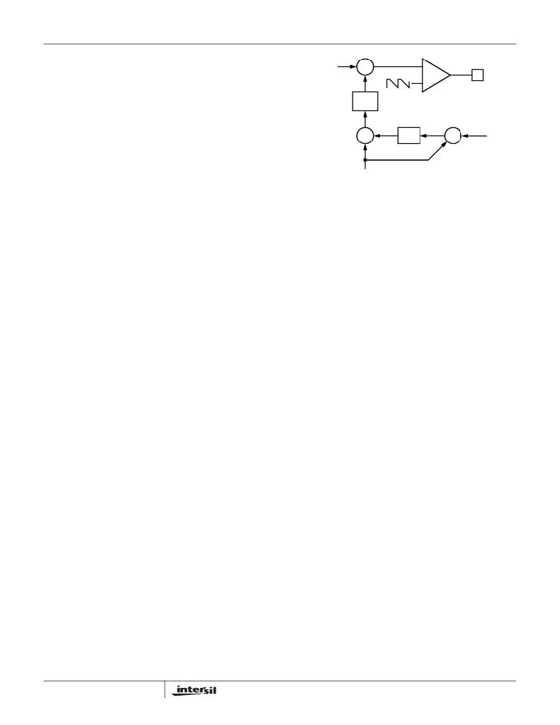
�The� circuitry� shown� in� Figure� 4� represents� channel-1� of� a�
�two� channel� converter.� This� circuitry� is� repeated� for�
�channel-2� of� the� converter.� From� Figure� 4,� the� following�
�equation� for� channel-1� sampled� current,� I� 1� ,� is� derived�
�+�
�I� 1�
�FIGURE� 5.� CHANNEL-1� PWM� FUNCTION� AND�
�CURRENT-BALANCE� ADJUSTMENT�
�Two� considerations� designers� face� are� MOSFET� selection�
�and� inductor� design.� Both� are� significantly� improved� when�
�channel� currents� track� at� any� load� level.� The� need� for�
�complex� drive� schemes� for� multiple� MOSFETs,� exotic�
�I� 1� =� I� L1� ----------------------� )�
�r� DS� (� ON�
�R� ISEN�
�(EQ.� 3)�
�magnetic� materials,� and� expensive� heat� sinks� is� avoided.�
�Resulting� in� a� cost-effective� and� easy� to� implement� solution�
�relative� to� single-phase� conversion.� Channel� current� balance�
�where� I� L1� is� half� of� the� total� load� current.�
�If� r� DS(ON)� sensing� is� not� desired,� an� independent� current-�
�sense� resistor� in� series� with� the� lower� MOSFET� source� can�
�serve� as� a� sense� element.�
�Channel-Current� Balance�
�The� sampled� current� from� both� channels,� I� 1� and� I� 2� ,� is� used�
�to� gauge� both� overall� load� current� and� the� relative� channel�
�current� carried� in� each� leg� of� the� converter.� The� individual�
�sample� currents� are� averaged.� The� resulting� average�
�current,� I� AVG� ,� provides� a� measure� of� the� total� load� current�
�demand� on� the� converter� and� the� appropriate� level� of�
�channel� current.� Using� Figures� 4� and� 5,� the� average� current�
�is� defined� as�
�insures� the� thermal� advantage� of� multi-phase� conversion� is�
�realized.� Heat� dissipation� is� spread� over� multiple� channels�
�and� a� greater� area� than� single� phase� approaches.�
�In� some� circumstances,� it� may� be� necessary� to� deliberately�
�design� some� channel-current� unbalance� into� the� system.� In�
�a� highly� compact� design,� one� channel� may� be� able� to� cool�
�more� effectively� than� the� other� due� to� nearby� air� flow� or� heat�
�sinking� components.� The� other� channel� may� have� more�
�difficulty� cooling� with� comparatively� less� air� flow� and� heat�
�sinking.� The� hotter� channel� may� also� be� located� close� to�
�other� heat-generating� components� tending� to� drive� it’s�
�temperature� even� higher.� In� these� cases,� the� proper�
�selection� of� the� current� sense� resistors� (R� ISEN� in� Figure� 4)�
�introduces� channel� current� unbalance� into� the� system.�
�I� AVG� =� ---------------� 2� -�
�I� 1� +� I�
�2�
�(EQ.� 4)�
�Increasing� the� value� of� R� ISEN� in� the� cooler� channel� and�
�decreasing� it� in� the� hotter� channel� moves� both� channels� into�
�I� AVG� =� -------------� ----------------------� )�
�R� ISEN�
�I� OUT� r� DS� (� ON�
�2�
�where� I� OUT� is� the� total� load� current.�
�The� average� current� is� then� subtracted� from� the� individual�
�channel� sample� currents.� The� resulting� error� current,� I� ER� ,� is�
�then� filtered� before� it� adjusts� V� COMP� .� The� modified� V� COMP�
�signal� is� compared� to� a� sawtooth� ramp� signal� and� produces�
�a� pulse� width� which� corrects� for� any� unbalance� and� drives�
�the� error� current� toward� zero.� Figure� 5� illustrates� Intersil’s�
�patented� current� balance� method� as� implemented� on� one�
�channel� of� a� multi-phase� converter.�
�10�
�thermal� balance� at� the� expense� of� current� balance.�
�Voltage� Regulation�
�The� output� of� the� error� amplifier,� V� COMP� ,� is� compared� to� the�
�sawtooth� waveform� to� modulate� the� pulse� width� of� the� PWM�
�signals.� The� PWM� signals� control� the� timing� of� the� Intersil�
�MOSFET� drivers� and� regulate� the� converter� output� to� the�
�specified� reference� voltage.� Three� distinct� inputs� to� the� error�
�amplifier� determine� the� voltage� level� of� V� COMP� .� The� internal�
�and� external� circuitry� which� control� voltage� regulation� is�
�illustrated� in� Figure� 6.�
�FN9085.7�
�December� 29,� 2004�
�相关PDF资料 |
PDF描述 |
|---|---|
| ISL6571CRZ | IC MOSF DRVR/SYNC SW COMPL 68QFN |
| ISL6611AIRZ | IC REG CTRLR DOUBLER PWM 16-QFN |
| ISL6617IRZ | IC PWM DOUBLER MONITOR 10DFN |
| ISL6627IRZ-T | IC CONTROLLER VR11.1 VR12 10DFN |
| ISL6719ARZ-T | IC REG LDO ADJ .1A 9-DFN |
相关代理商/技术参数 |
参数描述 |
|---|---|
| ISL6569CRZ | 功能描述:IC REG CTRLR DIVIDER PWM 32-QFN RoHS:是 类别:集成电路 (IC) >> PMIC - 稳压器 - DC DC 切换控制器 系列:- 产品培训模块:Lead (SnPb) Finish for COTS Obsolescence Mitigation Program 标准包装:2,500 系列:- PWM 型:电流模式 输出数:1 频率 - 最大:275kHz 占空比:50% 电源电压:18 V ~ 110 V 降压:无 升压:无 回扫:无 反相:无 倍增器:无 除法器:无 Cuk:无 隔离:是 工作温度:-40°C ~ 85°C 封装/外壳:8-SOIC(0.154",3.90mm 宽) 包装:带卷 (TR) |
| ISL6569CRZ-T | 功能描述:IC REG CTRLR DIVIDER PWM 32-QFN RoHS:是 类别:集成电路 (IC) >> PMIC - 稳压器 - DC DC 切换控制器 系列:- 产品培训模块:Lead (SnPb) Finish for COTS Obsolescence Mitigation Program 标准包装:2,500 系列:- PWM 型:电流模式 输出数:1 频率 - 最大:275kHz 占空比:50% 电源电压:18 V ~ 110 V 降压:无 升压:无 回扫:无 反相:无 倍增器:无 除法器:无 Cuk:无 隔离:是 工作温度:-40°C ~ 85°C 封装/外壳:8-SOIC(0.154",3.90mm 宽) 包装:带卷 (TR) |
| ISL6571CR | 制造商:Rochester Electronics LLC 功能描述:- Bulk 制造商:Intersil Corporation 功能描述: |
| ISL6571CR-T | 制造商:Rochester Electronics LLC 功能描述:- Bulk |
| ISL6571CRZ | 功能描述:IC MOSF DRVR/SYNC SW COMPL 68QFN RoHS:是 类别:集成电路 (IC) >> PMIC - MOSFET,电桥驱动器 - 内部开关 系列:- 标准包装:1,000 系列:- 类型:高端/低端驱动器 输入类型:SPI 输出数:8 导通状态电阻:850 毫欧,1.6 欧姆 电流 - 输出 / 通道:205mA,410mA 电流 - 峰值输出:500mA,1A 电源电压:9 V ~ 16 V 工作温度:-40°C ~ 150°C 安装类型:表面贴装 封装/外壳:20-SOIC(0.295",7.50mm 宽) 供应商设备封装:PG-DSO-20-45 包装:带卷 (TR) |
发布紧急采购,3分钟左右您将得到回复。