参数资料
| 型号: | ISL6569CR-T |
| 厂商: | Intersil |
| 文件页数: | 12/22页 |
| 文件大小: | 0K |
| 描述: | IC REG CTRLR DIVIDER PWM 32-QFN |
| 标准包装: | 6,000 |
| PWM 型: | 控制器 |
| 输出数: | 1 |
| 频率 - 最大: | 2MHz |
| 占空比: | 75% |
| 电源电压: | 4.75 V ~ 5.25 V |
| 降压: | 是 |
| 升压: | 无 |
| 回扫: | 无 |
| 反相: | 无 |
| 倍增器: | 无 |
| 除法器: | 是 |
| Cuk: | 无 |
| 隔离: | 无 |
| 工作温度: | 0°C ~ 70°C |
| 封装/外壳: | 32-VFQFN 裸露焊盘 |
| 包装: | 带卷 (TR) |
�� �
�
�ISL6569�
�ance� of� the� ISL6569� to� include� all� variations� in� current�
�sources,� amplifiers� and� the� reference� so� that� the� output� volt-�
�age� remains� within� the� specified� system� tolerance� of� ±� 1� %�
�over� temperature.�
�LOAD-LINE� REGULATION�
�Microprocessor� load� current� demands� change� from� near� no-�
�load� to� full� load� often� during� operation.� The� resulting� sizable�
�transient� current� slew� rate� causes� an� output� voltage� spike�
�since� the� converter� is� not� able� to� respond� fast� enough� to� the�
�rapidly� changing� current� demands.� The� magnitude� of� the�
�spike� is� dictated� by� the� ESR� and� ESL� of� the� output�
�capacitors� selected.� In� order� to� drive� the� cost� of� the� output�
�capacitor� solution� down,� one� commonly� accepted� approach�
�is� active� voltage� positioning.� By� adding� a� well� controlled�
�output� impedance,� the� output� voltage� can� effectively� be� level�
�shifted� in� a� direction� which� works� against� the� voltage� spike.�
�The� average� current� of� all� the� active� channels,� I� AVG� ,� flows�
�out� IOUT,� see� Figure� 6.� IOUT� is� connected� to� FB� through� a�
�load-line� regulation� resistor,� R� FB� .� The� resulting� voltage� drop�
�across� R� FB� is� proportional� to� the� output� current,� effectively�
�creating� an� output� voltage� droop� with� a� steady-state� value�
�defined� as�
�DYNAMIC� VID�
�Next� generation� microprocessors� can� change� VID� inputs� at�
�any� time� while� the� regulator� is� in� operation.� The� power�
�management� solution� is� required� to� monitor� the� DAC� inputs�
�and� respond� to� VID� voltage� transitions,� or� ‘on-the-fly’� VID�
�changes,� in� a� controlled� manner.� Supervising� the� safe� output�
�voltage� transition� within� the� DAC� range� of� the� processor�
�without� discontinuity� or� disruption.�
�The� ISL6569� checks� the� five� VID� inputs� at� the� beginning� of�
�each� channel-1� switching� cycle.� If� the� VID� code� has�
�changed,� the� controller� waits� one� complete� switching� cycle�
�to� validate� the� new� code.� If� the� VID� code� is� stable� for� this�
�entire� switching� cycle,� then� the� controller� will� begin� executing�
�the� output� voltage� change.� The� controller� begins�
�incrementing� the� reference� voltage� by� making� 25mV� steps�
�every� two� switching� cycles� until� it� reaches� the� new� VID� code.�
�The� total� time� required� for� a� VID� change,� t� DV� ,� is� dependent�
�on� the� switching� frequency� (f� S� ),� the� size� of� the� change�
�(� ?� VID),� and� the� time� before� the� next� switching� cycle� begins.�
�Since� the� ISL6569� recognizes� VID-code� changes� only� at� the�
�beginning� of� switching� cycles,� up� to� one� full� cycle� may� pass�
�before� a� VID� change� registers.� This� is� followed� by� a�
�V� DROOP� =� I� AVG� R� FB�
�(EQ.� 5)�
�one-cycle� wait� before� the� output� voltage� begins� to� change.�
�The� one-cycle� uncertainty� in� Equation� 8� is� due� to� the�
�possibility� that� the� VID� code� change� may� occur� up� to� one� full�
�In� most� cases,� each� channel� uses� the� same� R� ISEN� value� to�
�cycle� before� being� recognized.�
�-----� ?� 2� ------------------� –� 1� ?� <� t� DV� ≤� -----� ?� 2� ------------------� ?�
�f� S� ?� 0.025�
�f� S� ?� 0.025� ?�
�sense� current.� A� more� complete� expression� for� V� DROOP� is�
�derived� by� combining� equations� 4� and� 5.�
�?�
�1� ?� VID� 1� ?� VID�
�(EQ.� 8)�
�V� DROOP� =� -------------� ----------------------� R� FB�
�R� ISEN�
�I� OUT� r� DS� (� ON� )�
�2�
�(EQ.� 6)�
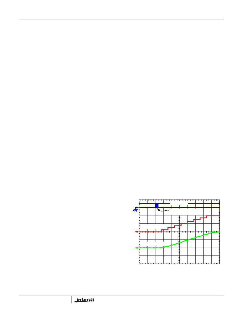
�The� time� required� for� a� converter� running� with� f� S� =� 500kHz� to�
�make� a� 1.2V� to� 1.4V� reference-voltage� change� is� between�
�Droop� is� an� optional� feature� of� the� ISL6569.� If� active� voltage�
�positioning� is� not� required,� simply� leave� the� IOUT� pin� open.�
�REFERENCE� OFFSET�
�30� μ� s� and� 32� μ� s� as� calculated� using� Equation� 8.� This� example�
�is� also� illustrated� in� Figure� 7.�
�Typical� microprocessor� tolerance� windows� are� centered�
�around� a� nominal� DAC� set� point.� Implementing� a� load-line�
�requires� offsetting� the� output� voltage� above� this� nominal�
�01110�
�00110�
�VID,� 5V/DIV�
�VID� CHANGE� OCCURS�
�ANYWHERE� HERE�
�DAC� set� point;� centering� the� load-line� within� the� static�
�specification� window.� The� ISL6569� features� an� internal�
�100� μ� A� current� source� which� feeds� out� the� OFS� pin.� Placing�
�a� resistor� from� OFS� and� ground� allows� the� user� to� set� the�
�amount� of� positive� offset� desired� directly� to� the� reference�
�1.2V�
�V� REF� ,� 100mV/DIV�
�voltage.� The� voltage� developed� across� the� OFS� resistor,�
�R� OFS� ,� is� divided� down� internally� by� a� factor� of� 10� and� directly�
�counters� the� DAC� voltage� at� the� error� amplifier� non-inverting�
�input.� Select� the� resistor� value� based� on� the� voltage� offset�
�desired,� V� OFS� ,� using� Equation� 7.�
�1.2V�
�V� OUT� ,� 100mV/DIV�
�V� OFS� ?� 10�
�R� OFS� =� ---------------------------�
�100� μ� A�
�12�
�(EQ.� 7)�
�5� μ� s/DIV�
�FIGURE� 7.� DYNAMIC-VID� WAVEFORMS� FOR� 500kHz� ISL6569�
�BASED� MULTI-PHASE� BUCK� CONVERTER�
�FN9085.7�
�December� 29,� 2004�
�相关PDF资料 |
PDF描述 |
|---|---|
| ISL6571CRZ | IC MOSF DRVR/SYNC SW COMPL 68QFN |
| ISL6611AIRZ | IC REG CTRLR DOUBLER PWM 16-QFN |
| ISL6617IRZ | IC PWM DOUBLER MONITOR 10DFN |
| ISL6627IRZ-T | IC CONTROLLER VR11.1 VR12 10DFN |
| ISL6719ARZ-T | IC REG LDO ADJ .1A 9-DFN |
相关代理商/技术参数 |
参数描述 |
|---|---|
| ISL6569CRZ | 功能描述:IC REG CTRLR DIVIDER PWM 32-QFN RoHS:是 类别:集成电路 (IC) >> PMIC - 稳压器 - DC DC 切换控制器 系列:- 产品培训模块:Lead (SnPb) Finish for COTS Obsolescence Mitigation Program 标准包装:2,500 系列:- PWM 型:电流模式 输出数:1 频率 - 最大:275kHz 占空比:50% 电源电压:18 V ~ 110 V 降压:无 升压:无 回扫:无 反相:无 倍增器:无 除法器:无 Cuk:无 隔离:是 工作温度:-40°C ~ 85°C 封装/外壳:8-SOIC(0.154",3.90mm 宽) 包装:带卷 (TR) |
| ISL6569CRZ-T | 功能描述:IC REG CTRLR DIVIDER PWM 32-QFN RoHS:是 类别:集成电路 (IC) >> PMIC - 稳压器 - DC DC 切换控制器 系列:- 产品培训模块:Lead (SnPb) Finish for COTS Obsolescence Mitigation Program 标准包装:2,500 系列:- PWM 型:电流模式 输出数:1 频率 - 最大:275kHz 占空比:50% 电源电压:18 V ~ 110 V 降压:无 升压:无 回扫:无 反相:无 倍增器:无 除法器:无 Cuk:无 隔离:是 工作温度:-40°C ~ 85°C 封装/外壳:8-SOIC(0.154",3.90mm 宽) 包装:带卷 (TR) |
| ISL6571CR | 制造商:Rochester Electronics LLC 功能描述:- Bulk 制造商:Intersil Corporation 功能描述: |
| ISL6571CR-T | 制造商:Rochester Electronics LLC 功能描述:- Bulk |
| ISL6571CRZ | 功能描述:IC MOSF DRVR/SYNC SW COMPL 68QFN RoHS:是 类别:集成电路 (IC) >> PMIC - MOSFET,电桥驱动器 - 内部开关 系列:- 标准包装:1,000 系列:- 类型:高端/低端驱动器 输入类型:SPI 输出数:8 导通状态电阻:850 毫欧,1.6 欧姆 电流 - 输出 / 通道:205mA,410mA 电流 - 峰值输出:500mA,1A 电源电压:9 V ~ 16 V 工作温度:-40°C ~ 150°C 安装类型:表面贴装 封装/外壳:20-SOIC(0.295",7.50mm 宽) 供应商设备封装:PG-DSO-20-45 包装:带卷 (TR) |
发布紧急采购,3分钟左右您将得到回复。