参数资料
| 型号: | ISL6611AIRZ |
| 厂商: | Intersil |
| 文件页数: | 13/14页 |
| 文件大小: | 0K |
| 描述: | IC REG CTRLR DOUBLER PWM 16-QFN |
| 标准包装: | 75 |
| PWM 型: | 控制器 |
| 输出数: | 2 |
| 频率 - 最大: | 1MHz |
| 电源电压: | 4.5 V ~ 5.5 V |
| 降压: | 无 |
| 升压: | 无 |
| 回扫: | 无 |
| 反相: | 无 |
| 倍增器: | 是 |
| 除法器: | 无 |
| Cuk: | 无 |
| 隔离: | 无 |
| 工作温度: | -40°C ~ 85°C |
| 封装/外壳: | 16-VQFN 裸露焊盘 |
| 包装: | 管件 |
�� �
�
�ISL6611A�
�part,� connect� it� to� the� adjacent� net� (LGATE2/PHASE2)� can�
�reduce� trace� inductance.�
�?� Shorten� all� gate� drive� loops� (UGATE-PHASE� and�
�LGATE-PGND)� and� route� them� closely� spaced.�
�?� Minimize� the� inductance� of� the� PHASE� node.� Ideally,� the�
�source� of� the� upper� and� the� drain� of� the� lower� MOSFET�
�should� be� as� close� as� thermally� allowable.�
�?� Minimize� the� current� loop� of� the� output� and� input� power�
�trains.� Short� the� source� connection� of� the� lower� MOSFET�
�to� ground� as� close� to� the� transistor� pin� as� feasible.� Input�
�capacitors� (especially� ceramic� decoupling)� should� be�
�placed� as� close� to� the� drain� of� upper� and� source� of� lower�
�MOSFETs� as� possible.�
�?� Avoid� routing� relatively� high� impedance� nodes� (such� as�
�PWM� and� ENABLE� lines)� close� to� high� dV/dt� UGATE� and�
�C� DS� /C� GS� ratio,� and� a� lower� gate-source� threshold� upper�
�FET� will� require� a� smaller� resistor� to� diminish� the� effect� of�
�the� internal� capacitive� coupling.� For� most� applications,� the�
�integrated� 20k� Ω� typically� sufficient,� not� affecting� normal�
�performance� and� efficiency.�
�The� coupling� effect� can� be� roughly� estimated� with� the�
�equations� in� Equation� 7,� which� assume� a� fixed� linear� input�
�ramp� and� neglect� the� clamping� effect� of� the� body� diode� of�
�the� upper� drive� and� the� bootstrap� capacitor.� Other� parasitic�
�components� such� as� lead� inductances� and� PCB�
�capacitances� are� also� not� taken� into� account.� These�
�equations� are� provided� for� guidance� purposes� only.� Thus,�
�the� actual� coupling� effect� should� be� examined� using� a� very�
�high� impedance� (10M� Ω� or� greater)� probe� to� ensure� a� safe�
�design� margin.�
�DS�
�?�
�----------------------------------� ?�
�?� dV� ?�
�V� GS_MILLER� =� -------� ?� R� ?� C� rss� ?� 1� –� e� dt�
�iss� ?�
�-------� ?� R� ?� C�
�PHASE� nodes.�
�In� addition,� connecting� the� thermal� pad� of� the� QFN� package�
�to� the� power� ground� through� multiple� vias,� or� placing� a� low�
�noise� copper� plane� (such� as� power� ground)� underneath� the�
�dV�
�–� V�
�dt� ?� ?�
�?� ?�
�?� ?�
�(EQ.� 7)�
�SOIC� part� is� recommended.� This� is� to� improve� heat�
�dissipation� and� allow� the� part� to� achieve� its� full� thermal�
�R� =� R� UGPH� +� R� GI�
�C� rss� =� C� GD�
�C� iss� =� C� GD� +� C� GS�
�potential.�
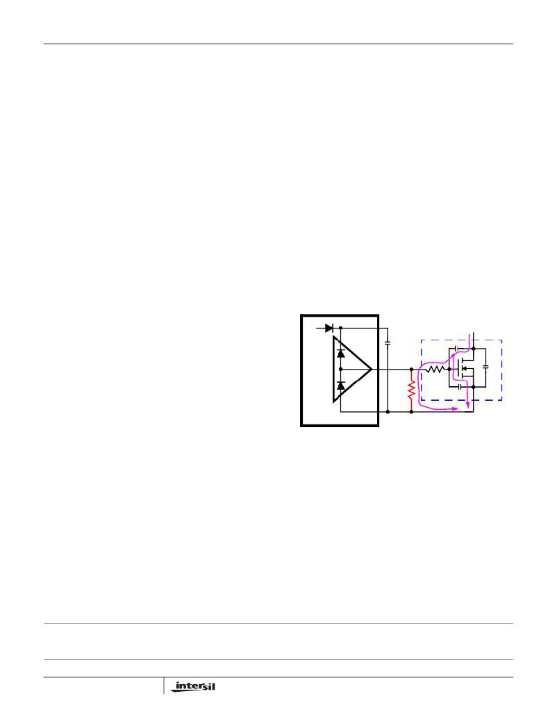
�Upper� MOSFET� Self� Turn-On� Effects� At� Start-up�
�Should� the� driver� have� insufficient� bias� voltage� applied,� its�
�outputs� are� floating.� If� the� input� bus� is� energized� at� a� high�
�VCC�
�BOOT�
�C� BOOT�
�VIN�
�D�
�dV/dt� rate� while� the� driver� outputs� are� floating,� due� to� the�
�C� GD�
�self-coupling� via� the� internal� C� GD� of� the� MOSFET,� the�
�UGATE� could� momentarily� rise� up� to� a� level� greater� than� the�
�threshold� voltage� of� the� MOSFET.� This� could� potentially� turn�
�DU�
�DL�
�UGATE�
�G�
�R� GI�
�C� DS�
�on� the� upper� switch� and� result� in� damaging� in-rush� energy.�
�Therefore,� if� such� a� situation� (when� input� bus� powered� up�
�before� the� bias� of� the� controller� and� driver� is� ready)� could�
�conceivably� be� encountered,� it� is� common� practice� to� place�
�PHASE�
�C� GS�
�S�
�Q� UPPER�
�a� resistor� (R� UGPH� )� across� the� gate� and� source� of� the� upper�
�MOSFET� to� suppress� the� Miller� coupling� effect.� The� value� of�
�FIGURE� 9.� GATE� TO� SOURCE� RESISTOR� TO� REDUCE�
�UPPER� MOSFET� MILLER� COUPLING�
�the� resistor� depends� mainly� on� the� input� voltage’s� rate� of�
�rise,� the� C� GD� /C� GS� ratio,� as� well� as� the� gate-source�
�threshold� of� the� upper� MOSFET.� A� higher� dV/dt,� a� lower�
�All� Intersil� U.S.� products� are� manufactured,� assembled� and� tested� utilizing� ISO9000� quality� systems.�
�Intersil� Corporation’s� quality� certifications� can� be� viewed� at� www.intersil.com/design/quality�
�Intersil� products� are� sold� by� description� only.� Intersil� Corporation� reserves� the� right� to� make� changes� in� circuit� design,� software� and/or� specifications� at� any� time� without�
�notice.� Accordingly,� the� reader� is� cautioned� to� verify� that� data� sheets� are� current� before� placing� orders.� Information� furnished� by� Intersil� is� believed� to� be� accurate� and�
�reliable.� However,� no� responsibility� is� assumed� by� Intersil� or� its� subsidiaries� for� its� use;� nor� for� any� infringements� of� patents� or� other� rights� of� third� parties� which� may� result�
�from� its� use.� No� license� is� granted� by� implication� or� otherwise� under� any� patent� or� patent� rights� of� Intersil� or� its� subsidiaries.�
�For� information� regarding� Intersil� Corporation� and� its� products,� see� www.intersil.com�
�13�
�FN6881.1�
�August� 28,� 2012�
�相关PDF资料 |
PDF描述 |
|---|---|
| ISL6617IRZ | IC PWM DOUBLER MONITOR 10DFN |
| ISL6627IRZ-T | IC CONTROLLER VR11.1 VR12 10DFN |
| ISL6719ARZ-T | IC REG LDO ADJ .1A 9-DFN |
| ISL6720AARZ | IC REG LDO 5V/ADJ 11-DFN |
| ISL6721AAVZ | IC REG CTRLR PWM CM 16-TSSOP |
相关代理商/技术参数 |
参数描述 |
|---|---|
| ISL6611AIRZ-T | 功能描述:IC REG CTRLR DOUBLER PWM 16-QFN RoHS:是 类别:集成电路 (IC) >> PMIC - 稳压器 - DC DC 切换控制器 系列:- 产品培训模块:Lead (SnPb) Finish for COTS Obsolescence Mitigation Program 标准包装:2,500 系列:- PWM 型:电流模式 输出数:1 频率 - 最大:275kHz 占空比:50% 电源电压:18 V ~ 110 V 降压:无 升压:无 回扫:无 反相:无 倍增器:无 除法器:无 Cuk:无 隔离:是 工作温度:-40°C ~ 85°C 封装/外壳:8-SOIC(0.154",3.90mm 宽) 包装:带卷 (TR) |
| ISL6612ACB | 功能描述:IC MOSFET DRVR SYNC BUCK 8-SOIC RoHS:否 类别:集成电路 (IC) >> PMIC - MOSFET,电桥驱动器 - 外部开关 系列:- 标准包装:50 系列:- 配置:低端 输入类型:非反相 延迟时间:40ns 电流 - 峰:9A 配置数:1 输出数:1 高端电压 - 最大(自引导启动):- 电源电压:4.5 V ~ 35 V 工作温度:-40°C ~ 125°C 安装类型:表面贴装 封装/外壳:TO-263-6,D²Pak(5 引线+接片),TO-263BA 供应商设备封装:TO-263 包装:管件 |
| ISL6612ACB-T | 功能描述:IC MOSFET DRVR SYNC BUCK 8-SOIC RoHS:否 类别:集成电路 (IC) >> PMIC - MOSFET,电桥驱动器 - 外部开关 系列:- 标准包装:50 系列:- 配置:低端 输入类型:非反相 延迟时间:40ns 电流 - 峰:9A 配置数:1 输出数:1 高端电压 - 最大(自引导启动):- 电源电压:4.5 V ~ 35 V 工作温度:-40°C ~ 125°C 安装类型:表面贴装 封装/外壳:TO-263-6,D²Pak(5 引线+接片),TO-263BA 供应商设备封装:TO-263 包装:管件 |
| ISL6612ACBZ | 功能描述:IC DRIVER MOSFET SYNC BUCK 8SOIC RoHS:是 类别:集成电路 (IC) >> PMIC - MOSFET,电桥驱动器 - 外部开关 系列:- 标准包装:95 系列:- 配置:高端和低端,独立 输入类型:非反相 延迟时间:160ns 电流 - 峰:290mA 配置数:1 输出数:2 高端电压 - 最大(自引导启动):600V 电源电压:10 V ~ 20 V 工作温度:-40°C ~ 125°C 安装类型:表面贴装 封装/外壳:8-SOIC(0.154",3.90mm 宽) 供应商设备封装:8-SOIC 包装:管件 产品目录页面:1381 (CN2011-ZH PDF) |
| ISL6612ACBZA | 功能描述:IC MOSFET DRVR SYNC BUCK 8-SOIC RoHS:是 类别:集成电路 (IC) >> PMIC - MOSFET,电桥驱动器 - 外部开关 系列:- 标准包装:6,000 系列:* |
发布紧急采购,3分钟左右您将得到回复。