- 您现在的位置:买卖IC网 > PDF目录20670 > ISL8104EVAL2Z (Intersil)EVAL BOARD 2 FOR ISL8104 PDF资料下载
参数资料
| 型号: | ISL8104EVAL2Z |
| 厂商: | Intersil |
| 文件页数: | 10/14页 |
| 文件大小: | 0K |
| 描述: | EVAL BOARD 2 FOR ISL8104 |
| 标准包装: | 1 |
| 系列: | * |
�� �
�
�ISL8104�
�times� f� SW� ).� f� SW� represents� the� switching� frequency� of� the�
�regulator.� Change� the� numerical� factor� (0.7)� below� to�
�reflect� desired� placement� of� this� pole.� Placement� of� F� P2�
�lower� in� frequency� helps� reduce� the� gain� of� the�
�compensation� network� at� high� frequency,� in� turn� reducing�
�the� HF� ripple� component� at� the� COMP� pin� and� minimizing�
�resultant� duty� cycle� jitter.�
�phase� margin.� The� mathematical� model� presented� makes� a�
�number� of� approximations� and� is� generally� not� accurate� at�
�frequencies� approaching� or� exceeding� half� the� switching�
�frequency.� When� designing� compensation� networks,� select�
�target� crossover� frequencies� in� the� range� of� 10%� to� 30%� of�
�the� switching� frequency,� f� SW� .�
�R� 3� =� --------------------�
�f� SW�
�C� 3� =� -----------------------------------------------�
�R� 1�
�-----------� –� 1�
�F� LC�
�1�
�2� π� ?� R� 3� ?� 0.7� ?� f� SW�
�(EQ.� 12)�
�F� Z1� F� Z2�
�F� P1�
�MODULATOR� GAIN�
�COMPENSATION� GAIN�
�CLOSED� LOOP� GAIN�
�OPEN� LOOP� E/A� GAIN�
�F� P2�
�It� is� recommended� that� a� mathematical� model� be� used� to�
�20� log� ?� --------� ?�
�MAX� ?� V� IN�
�OSC�
�plot� the� loop� response.� Check� the� loop� gain� against� the� error�
�amplifier� ’s� open-loop� gain.� Verify� phase� margin� results� and�
�adjust� as� necessary.� Equation� 13� describes� the� frequency�
�response� of� the� modulator� (G� MOD� ),� feedback� compensation�
�(G� FB� )� and� closed-loop� response� (G� CL� ):�
�0�
�R2�
�?� R1� ?�
�D�
�20� log� ----------------------------------�
�V�
�G� CL�
�G� FB�
�G� MOD� (� f� )� =� -------------------------------� ?� -----------------------------------------------------------------------------------------------------------�
�V� OSC�
�1� +� s� (� f� )� ?� (� ESR� +� DCR� )� ?� C� +� s� (� f� )� ?� L� ?� C�
�D� MAX� ?� V� IN� 1� +� s� (� f� )� ?� ESR� ?� C�
�2�
�LOG�
�F� LC�
�F� CE�
�F� 0�
�G� MOD�
�FREQUENCY�
�G� FB� (� f� )� =� ----------------------------------------------------� ?�
�1� +� s� (� f� )� ?� (� R� 1� +� R� 3� )� ?� C� 3�
�(� 1� +� s� (� f� )� ?� R� 3� ?� C� 3� )� ?� ?� 1� +� s� (� f� )� ?� R� 2� ?� ?� ---------------------� ?� ?�
�1� +� s� (� f� )� ?� R� 2� ?� C� 1�
�s� (� f� )� ?� R� 1� ?� (� C� 1� +� C� 2� )�
�-------------------------------------------------------------------------------------------------------------------------�
�?� ?� C� 1� ?� C� 2� ?� ?�
�?� ?� C� 1� +� C� 2� ?� ?�
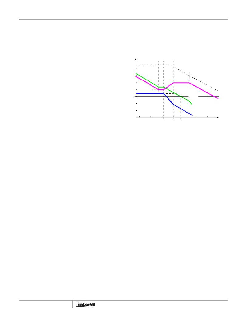
�FIGURE� 8.� ASYMPTOTIC� BODE� PLOT� OF� CONVERTER� GAIN�
�Component� Selection� Guidelines�
�Output� Capacitor� Selection�
�An� output� capacitor� is� required� to� filter� the� output� and� supply�
�the� load� transient� current.� The� filtering� requirements� are� a�
�G� CL� (� f� )� =� G� MOD� (� f� )� ?� G� FB� (� f� )�
�where� ,� s� (� f� )� =� 2� π� ?� f� ?� j�
�function� of� the� switching� frequency� and� the� ripple� current.�
�(EQ.� 13)�
�COMPENSATION� BREAK� FREQUENCY� EQUATIONS�
�The� load� transient� requirements� are� a� function� of� the� slew�
�rate� (di/dt)� and� the� magnitude� of� the� transient� load� current.�
�These� requirements� are� generally� met� with� a� mix� of�
�F� Z1� =� -------------------------------�
�F� P1� =� ---------------------------------------------�
�2� π� ?� R� 2� ?� ---------------------�
�1�
�2� π� ?� R� 2� ?� C� 1�
�1�
�C� 1� ?� C� 2�
�C� 1� +� C� 2�
�capacitors� and� careful� layout.�
�For� applications� that� have� transient� load� rates� above� 1A/ns,�
�high� frequency� capacitors� initially� supply� the� transient� and�
�F� Z2� =� -------------------------------------------------�
�F� P2� =� -------------------------------�
�1�
�2� π� ?� (� R� 1� +� R� 3� )� ?� C� 3�
�1�
�2� π� ?� R� 3� ?� C� 3�
�(EQ.� 14)�
�slow� the� current� load� rate� seen� by� the� bulk� capacitors.� The�
�bulk� filter� capacitor� values� are� generally� determined� by� the�
�Figure� 8� shows� an� asymptotic� plot� of� the� DC/DC� converter’s�
�gain� vs� frequency.� The� actual� Modulator� Gain� has� a� high� gain�
�peak� dependent� on� the� quality� factor� (Q)� of� the� output� filter,�
�which� is� not� shown.� Using� the� previously� mentioned� guidelines�
�should� yield� a� compensation� gain� similar� to� the� curve� plotted.�
�The� open� loop� error� amplifier� gain� bounds� the� compensation�
�gain.� Check� the� compensation� gain� at� F� P2� against� the�
�capabilities� of� the� error� amplifier.� The� closed� loop� gain,� G� CL� ,� is�
�constructed� on� the� log-log� graph� of� Figure� 8� by� adding� the�
�modulator� gain,� G� MOD� (in� dB),� to� the� feedback�
�compensation� gain,� G� FB� (in� dB).� This� is� equivalent� to�
�multiplying� the� modulator� transfer� function� and� the�
�compensation� transfer� function� and� then� plotting� the�
�resulting� gain.�
�A� stable� control� loop� has� a� gain� crossing� with� close� to� a�
�-20dB/decade� slope� and� a� phase� margin� greater� than� 45°.�
�Include� worst� case� component� variations� when� determining�
�10�
�ESR� (effective� series� resistance)� and� voltage� rating�
�requirements� rather� than� actual� capacitance� requirements.�
�High� frequency� decoupling� capacitors� should� be� placed� as�
�close� to� the� power� pins� of� the� load� as� physically� possible.� Be�
�careful� not� to� add� inductance� in� the� circuit� board� wiring� that�
�could� cancel� the� usefulness� of� these� low� inductance�
�components.� Consult� with� the� manufacturer� of� the� load� on�
�specific� decoupling� requirements.�
�Use� only� specialized� low-ESR� capacitors� intended� for�
�switching-regulator� applications� for� the� bulk� capacitors.�
�The� bulk� capacitor� ’s� ESR� will� determine� the� output� ripple�
�voltage� and� the� initial� voltage� drop� after� a� high� slew-rate�
�transient.� An� aluminum� electrolytic� capacitor's� ESR� value� is�
�related� to� the� case� size� with� lower� ESR� available� in� larger�
�case� sizes.� However,� the� equivalent� series� inductance�
�(ESL)� of� these� capacitors� increases� with� case� size� and� can�
�reduce� the� usefulness� of� the� capacitor� to� high� slew-rate�
�FN9257.2�
�March� 7,� 2008�
�相关PDF资料 |
PDF描述 |
|---|---|
| ISL6208CRZ-T | IC MOSFET DRVR SYNC BUCK 8-QFN |
| TC1313-1P0EMFTR | IC REG DL BUCK/LINEAR SYNC 10DFN |
| EBM11DRTH | CONN EDGECARD 22POS DIP .156 SLD |
| A7OXB-1506M | CABLE D-SUB - AFN15B/AE15M/X |
| VI-J6B-EW-B1 | CONVERTER MOD DC/DC 95V 100W |
相关代理商/技术参数 |
参数描述 |
|---|---|
| ISL8104IBZ | 功能描述:IC REG CTRLR BUCK PWM VM 14-SOIC RoHS:是 类别:集成电路 (IC) >> PMIC - 稳压器 - DC DC 切换控制器 系列:- 产品培训模块:Lead (SnPb) Finish for COTS Obsolescence Mitigation Program 标准包装:2,500 系列:- PWM 型:电流模式 输出数:1 频率 - 最大:275kHz 占空比:50% 电源电压:18 V ~ 110 V 降压:无 升压:无 回扫:无 反相:无 倍增器:无 除法器:无 Cuk:无 隔离:是 工作温度:-40°C ~ 85°C 封装/外壳:8-SOIC(0.154",3.90mm 宽) 包装:带卷 (TR) |
| ISL8104IBZ | 制造商:Intersil Corporation 功能描述:Pulse Width Modulation (PWM) Controller |
| ISL8104IBZ-T | 功能描述:IC REG CTRLR BUCK PWM VM 14-SOIC RoHS:是 类别:集成电路 (IC) >> PMIC - 稳压器 - DC DC 切换控制器 系列:- 产品培训模块:Lead (SnPb) Finish for COTS Obsolescence Mitigation Program 标准包装:2,500 系列:- PWM 型:电流模式 输出数:1 频率 - 最大:275kHz 占空比:50% 电源电压:18 V ~ 110 V 降压:无 升压:无 回扫:无 反相:无 倍增器:无 除法器:无 Cuk:无 隔离:是 工作温度:-40°C ~ 85°C 封装/外壳:8-SOIC(0.154",3.90mm 宽) 包装:带卷 (TR) |
| ISL8104IRZ | 功能描述:IC REG CTRLR BUCK PWM VM 16-QFN RoHS:是 类别:集成电路 (IC) >> PMIC - 稳压器 - DC DC 切换控制器 系列:- 产品培训模块:Lead (SnPb) Finish for COTS Obsolescence Mitigation Program 标准包装:2,500 系列:- PWM 型:电流模式 输出数:1 频率 - 最大:275kHz 占空比:50% 电源电压:18 V ~ 110 V 降压:无 升压:无 回扫:无 反相:无 倍增器:无 除法器:无 Cuk:无 隔离:是 工作温度:-40°C ~ 85°C 封装/外壳:8-SOIC(0.154",3.90mm 宽) 包装:带卷 (TR) |
| ISL8104IRZ-T | 功能描述:IC REG CTRLR BUCK PWM VM 16-QFN RoHS:是 类别:集成电路 (IC) >> PMIC - 稳压器 - DC DC 切换控制器 系列:- 产品培训模块:Lead (SnPb) Finish for COTS Obsolescence Mitigation Program 标准包装:2,500 系列:- PWM 型:电流模式 输出数:1 频率 - 最大:275kHz 占空比:50% 电源电压:18 V ~ 110 V 降压:无 升压:无 回扫:无 反相:无 倍增器:无 除法器:无 Cuk:无 隔离:是 工作温度:-40°C ~ 85°C 封装/外壳:8-SOIC(0.154",3.90mm 宽) 包装:带卷 (TR) |
发布紧急采购,3分钟左右您将得到回复。