- 您现在的位置:买卖IC网 > Datasheet目录466 > JN5139/001,531 (NXP Semiconductors)MCU 802.15.4 32BIT 2.4G 56-QFN Datasheet资料下载
参数资料
| 型号: | JN5139/001,531 |
| 厂商: | NXP Semiconductors |
| 文件页数: | 31/82页 |
| 文件大小: | 0K |
| 描述: | MCU 802.15.4 32BIT 2.4G 56-QFN |
| 标准包装: | 500 |
| 系列: | JN5139-001Rx |
| 频率: | 2.4GHz |
| 调制或协议: | 802.15.4 Zigbee |
| 应用: | 通用 |
| 功率 - 输出: | 3dBm |
| 灵敏度: | -96dBm |
| 电源电压: | 2.7 V ~ 3.6 V |
| 电流 - 接收: | 37mA |
| 电流 - 传输: | 37mA |
| 数据接口: | PCB,表面贴装 |
| 存储容量: | 96kB RAM,192kB ROM |
| 天线连接器: | PCB,表面贴装 |
| 工作温度: | -40°C ~ 85°C |
| 封装/外壳: | 56-VFQFN |
| 包装: | 带卷 (TR) |
第1页第2页第3页第4页第5页第6页第7页第8页第9页第10页第11页第12页第13页第14页第15页第16页第17页第18页第19页第20页第21页第22页第23页第24页第25页第26页第27页第28页第29页第30页当前第31页第32页第33页第34页第35页第36页第37页第38页第39页第40页第41页第42页第43页第44页第45页第46页第47页第48页第49页第50页第51页第52页第53页第54页第55页第56页第57页第58页第59页第60页第61页第62页第63页第64页第65页第66页第67页第68页第69页第70页第71页第72页第73页第74页第75页第76页第77页第78页第79页第80页第81页第82页
�� ��
��
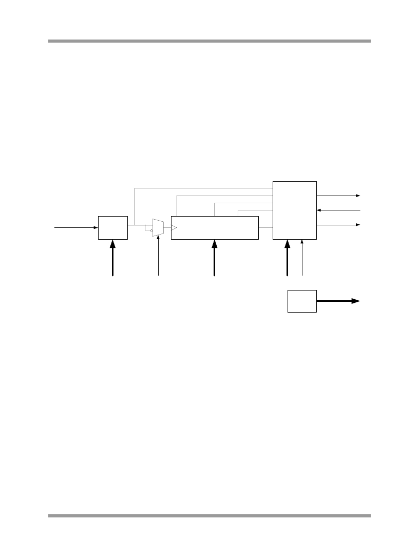
��10� Serial� Peripheral� Interface�
�The� Serial� Peripheral� Interface� (SPI)� allows� high-speed� synchronous� data� transfer� between� the� JN5139� and�
�peripheral� devices.� The� JN5139� operates� as� a� master� on� the� SPI� bus� and� all� other� devices� connected� to� the� SPI� are�
�expected� to� be� slave� devices� under� the� control� of� the� JN5139� CPU.� The� SPI� includes� the� following� features:�
�?�
�?�
�?�
�?�
�?�
�?�
�?�
�Full-duplex,� three-wire� synchronous� data� transfer�
�Programmable� bit� rates� up� to� 16Mbps�
�Programmable� transaction� size� of� 8,16� or� 32� bits�
�Supports� standard� SPI� modes� 0,� 1,� 2,� 3� to� allow� control� over� the� relationship� between� clock� and� transmit� /�
�receive� data�
�Automatic� slave� select� generation� (up� to� 5� slaves)�
�Maskable� transaction� complete� interrupt�
�LSB� First� or� MSB� First� Data� Transfer�
�SPICLK�
�SPI� Bus�
�Cycle�
�SPIMISO�
�16� MHz�
�Clock�
�Divider�
�31�
�15�
�Data� Buffer�
�7�
�0�
�Controller�
�SPIMOSI�
�Select�
�SPISEL� [4..0]�
�Latch�
�Figure� 22:� SPI� Block� Diagram�
�The� SPI� bus� employs� a� simple� shift� register� data� transfer� scheme.� Data� is� clocked� out� of� and� into� the� active� devices�
�in� a� first-in,� first-out� fashion� allowing� SPI� devices� to� transmit� and� receive� data� simultaneously.�
�There� are� three� dedicated� pins� SPICLK,� SPIMOSI,� SPIMISO� that� are� shared� across� all� devices� on� the� bus.� Master-�
�Out-Slave-In� or� Master-In-Slave-Out� data� transfer� is� relative� to� the� clock� signal� SPICLK� generated� by� the� JN5139.�
�The� JN5139� provides� five� slave� selects,� SPISEL0� to� SPISEL4� to� allow� five� SPI� peripherals� on� the� bus.� SPISEL0� is� a�
�dedicated� pin� and� SPISEL1� to� 4,� are� alternate� functions� of� pins� DIO0� to� 3� respectively.� This� allows� a� serial� flash�
�memory� to� be� connected� to� SPISEL0� and� download� to� internal� RAM� via� software� from� reset,� as� part� of� the� boot�
�process,� see� section� 4.4.�
�The� interface� can� transfer� 8,� 16� or� 32� bits� without� software� intervention� and� can� keep� the� slave� select� lines� asserted�
�between� transfers� when� required,� to� enable� longer� transfers� to� be� performed.�
�?� NXP� Laboratories� UK� 2010�
�JN-DS-JN5139� 1v9�
�31�
�相关PDF资料 |
PDF描述 |
|---|---|
| JN5139-EK000 | KIT EVAL IEEE802.15.4 JN5139 |
| JN5139/Z01,515 | IC MCU ZIGBEE 32BIT 2.4G 56QFN |
| JN5139-Z01-M/02R1V | MODULE ZIGBEE SMA CONN HP JN5139 |
| JN5148/001M04T,534 | MODULE ZIGBEE PRO HP U.FL CONN |
| JN5148-UG010 | KIT UPGRADE ZIGBEE PRO |
相关代理商/技术参数 |
参数描述 |
|---|---|
| JN5139-001-M/00R1T | 功能描述:Zigbee/802.15.4模块 WIRELESS MCU IEEE802.15.4 TRNSCVR RoHS:否 制造商:Digi International 频带:902 MHz to 928 MHz 视线范围: 数据速率: 灵敏度: 工作电源电压:2.4 V to 3.6 V 传输供电电流:215 mA 接收供电电流:26 mA 输出功率:250 mW 天线连接器类型:Wire 最大工作温度:+ 85 C 尺寸:32.94 mm x 22 mm x 2.03 mm |
| JN5139-001-M/01R1V | 功能描述:Zigbee/802.15.4模块 WIRELESS MCU IEEE802.15.4 TRNSCVR RoHS:否 制造商:Digi International 频带:902 MHz to 928 MHz 视线范围: 数据速率: 灵敏度: 工作电源电压:2.4 V to 3.6 V 传输供电电流:215 mA 接收供电电流:26 mA 输出功率:250 mW 天线连接器类型:Wire 最大工作温度:+ 85 C 尺寸:32.94 mm x 22 mm x 2.03 mm |
| JN5139-001-M/02R1V | 功能描述:Zigbee/802.15.4模块 WIRELESS MCU IEEE802.15.4 TRNSCVR RoHS:否 制造商:Digi International 频带:902 MHz to 928 MHz 视线范围: 数据速率: 灵敏度: 工作电源电压:2.4 V to 3.6 V 传输供电电流:215 mA 接收供电电流:26 mA 输出功率:250 mW 天线连接器类型:Wire 最大工作温度:+ 85 C 尺寸:32.94 mm x 22 mm x 2.03 mm |
| JN5139-001-M/03R1T | 功能描述:Zigbee/802.15.4模块 WIRELESS MCU IEEE802.15.4 TRNSCVR RoHS:否 制造商:Digi International 频带:902 MHz to 928 MHz 视线范围: 数据速率: 灵敏度: 工作电源电压:2.4 V to 3.6 V 传输供电电流:215 mA 接收供电电流:26 mA 输出功率:250 mW 天线连接器类型:Wire 最大工作温度:+ 85 C 尺寸:32.94 mm x 22 mm x 2.03 mm |
| JN5139-001-M/04R1T | 功能描述:Zigbee/802.15.4模块 WIRELESS MCU IEEE802.15.4 TRNSCVR RoHS:否 制造商:Digi International 频带:902 MHz to 928 MHz 视线范围: 数据速率: 灵敏度: 工作电源电压:2.4 V to 3.6 V 传输供电电流:215 mA 接收供电电流:26 mA 输出功率:250 mW 天线连接器类型:Wire 最大工作温度:+ 85 C 尺寸:32.94 mm x 22 mm x 2.03 mm |
发布紧急采购,3分钟左右您将得到回复。