- 您现在的位置:买卖IC网 > PDF目录1223 > KIT33887PNBEVB (Freescale Semiconductor)KIT EVAL 33887 5A H-BRIDGE PQFN PDF资料下载
参数资料
| 型号: | KIT33887PNBEVB |
| 厂商: | Freescale Semiconductor |
| 文件页数: | 11/37页 |
| 文件大小: | 0K |
| 描述: | KIT EVAL 33887 5A H-BRIDGE PQFN |
| 标准包装: | 1 |
| 主要目的: | 电源管理,H 桥驱动器(内部 FET) |
| 嵌入式: | 否 |
| 已用 IC / 零件: | MC33887 |
| 主要属性: | 5A 5 ~ 28V PWM 至 20kHz 有源电流限制 |
| 次要属性: | 故障状态,睡眠模式,比例电流镜像输出 |
| 已供物品: | 板,CD |
| 相关产品: | MC33887DWBR2-ND - IC H-BRIDGE 5A LOAD FDBK 54-SOIC MC33887VWR2-ND - IC H-BRIDGE 5.0A W/CS 20-HSOP MC33887PNBR2-ND - IC H-BRIDGE 5A CURR FDBK 36-PQFN MC33887PNB-ND - IC H-BRIDGE CURR FDBK 5A 36-PQFN MC33887DHR2-ND - IC H-BRIDGE 5A CURR FDBK 20-HSOP MC33887VW-ND - IC H-BRIDGE 5.0A W/CS 20-HSOP MC33887DWB-ND - IC H-BRIDGE 5.0A W/CS 54-SOIC MC33887DH-ND - IC H-BRIDGE 5.0A W/CS 20-HSOP |
第1页第2页第3页第4页第5页第6页第7页第8页第9页第10页当前第11页第12页第13页第14页第15页第16页第17页第18页第19页第20页第21页第22页第23页第24页第25页第26页第27页第28页第29页第30页第31页第32页第33页第34页第35页第36页第37页
�� �
�
�ELECTRICAL� CHARACTERISTICS�
�DYNAMIC� ELECTRICAL� CHARACTERISTICS�
�DYNAMIC� ELECTRICAL� CHARACTERISTICS�
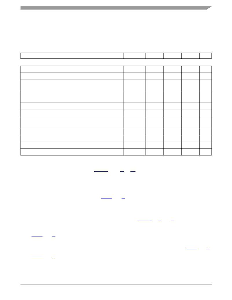
�Table� 5.� DYNAMIC� ELECTRICAL� CHARACTERISTICS�
�Characteristics� noted� under� conditions� 5.0� V� ≤� V+� ≤� 28� V� and� -40� °� C� ≤� T� A� ≤� 125� °� C� unless� otherwise� noted.� Typical� values�
�noted� reflect� the� approximate� parameter� mean� at� T� A� =� 25� °� C� under� nominal� conditions� unless� otherwise� noted.�
�Characteristic�
�Symbol�
�Min�
�Typ�
�Max�
�Unit�
�TIMING� CHARACTERISTICS�
�PWM� Frequency� (24)�
�f� PWM�
�–�
�10�
�–�
�kHz�
�Maximum� Switching� Frequency� During� Active� Current� Limiting�
�(25)�
�f� MAX�
�–�
�–�
�20�
�kHz�
�Output� ON� Delay� (26)�
�t� D� (ON)�
�μ� s�
�V+� =� 14� V�
�Output� OFF� Delay� (26)�
�V+� =� 14� V�
�t� D� (OFF)�
�–�
�–�
�–�
�–�
�18�
�18�
�μ� s�
�,�
�I� LIM� Output� Constant-OFF� Time� for� Low-Side� MOSFETs�
�I� LIM� Blanking� Time� for� Low-Side� MOSFETs� (29)� ,� (28)�
��t� A�
�t� B�
�15�
�12�
�20.5�
�16.5�
�26�
�21�
�μ� s�
�μ� s�
�Output� Rise� and� Fall� Time� (30)�
�t� F� ,� t� R�
�μ� s�
�V+� =� 14� V,� I� OUT� =� 3.0� A�
�2.0�
�5.0�
�8.0�
�Disable� Delay� Time� (31)�
�t� D� (DISABLE)�
�–�
�–�
�8.0�
�μ� s�
�Power-ON� Delay� Time�
�(32)�
�t� POD�
�–�
�1.0�
�5.0�
�ms�
�Wake-Up� Delay� Time� (32)�
�t� WUD�
�–�
�1.0�
�5.0�
�ms�
�Output� MOSFET� Body� Diode� Reverse� Recovery� Time�
�(33)�
�t� RR�
�100�
�–�
�–�
�ns�
�Notes�
�24� The� outputs� can� be� PWM-controlled� from� an� external� source.� This� is� typically� done� by� holding� one� input� high� while� applying� a� PWM�
�pulse� train� to� the� other� input.� The� maximum� PWM� frequency� obtainable� is� a� compromise� between� switching� losses� and� switching�
�frequency.� See� Typical� Switching� Waveforms,� Figures 12� through� 19� ,� pp.� 14–� 17.�
�25� The� Maximum� Switching� Frequency� during� active� current� limiting� is� internally� implemented.� The� internal� current� limit� circuitry� produces�
�a� constant-OFF-time� pulse-width� modulation� of� the� output� current.� The� output� load’s� inductance,� capacitance,� and� resistance�
�characteristics� affect� the� total� switching� period� (OFF-time� +� ON-time)� and� thus� the� PWM� frequency� during� current� limit.�
�26� Output� Delay� is� the� time� duration� from� the� midpoint� of� the� IN1� or� IN2� input� signal� to� the� 10%� or� 90%� point� (dependent� on� the� transition�
�direction)� of� the� OUT1� or� OUT2� signal.� If� the� output� is� transitioning� HIGH-to-LOW,� the� delay� is� from� the� midpoint� of� the� input� signal� to�
�the� 90%� point� of� the� output� response� signal.� If� the� output� is� transitioning� LOW-to-HIGH,� the� delay� is� from� the� midpoint� of� the� input� signal�
��27� I� LIM� Output� Constant-OFF� Time� is� the� time� during� which� the� internal� constant-OFF� time� PWM� current� regulation� circuit� has� tri-stated�
�the� output� bridge.�
�28� Load� currents� ramping� up� to� the� current� regulation� threshold� become� limited� at� the� I� LIM� value.� The� short� circuit� currents� possess� a� di/dt�
�that� ramps� up� to� the� I� SCH� or� I� SCL� threshold� during� the� I� LIM� blanking� time,� registering� as� a� short� circuit� event� detection� and� causing� the�
�shutdown� circuitry� to� force� the� output� into� an� immediate� tri-state� latch-OFF.� See� Figures 10� and� 11� ,� page� 13� .� Operation� in� Current� Limit�
�mode� may� cause� junction� temperatures� to� rise.� Junction� temperatures� above� ~160� °� C� will� cause� the� output� current� limit� threshold� to�
�progressively� “fold� back”,� or� decrease� with� temperature,� until� ~175� °� C� is� reached,� after� which� the� T� LIM� thermal� latch-OFF� will� occur.�
�Permissible� operation� within� this� fold-back� region� is� limited� to� nonrepetitive� transient� events� of� duration� not� to� exceed� 30� seconds.� See�
��29� I� LIM� Blanking� Time� is� the� time� during� which� the� current� regulation� threshold� is� ignored� so� that� the� short-circuit� detection� threshold�
�comparators� may� have� time� to� act.�
�30� Rise� Time� is� from� the� 10%� to� the� 90%� level� and� Fall� Time� is� from� the� 90%� to� the� 10%� level� of� the� output� signal.� See� Figure 8� ,� page� 12� .�
�31� Disable� Delay� Time� is� the� time� duration� from� the� midpoint� of� the� D� (disable)� input� signal� to� 10%� of� the� output� tri-state� response.� See�
��32� Parameter� has� been� characterized� but� not� production� tested.�
�33� Parameter� is� guaranteed� by� design� but� not� production� tested.�
�33887�
�Analog� Integrated� Circuit� Device� Data�
�Freescale� Semiconductor�
�11�
�相关PDF资料 |
PDF描述 |
|---|---|
| KIT33905D5EKEVBE | KIT EVALUATION FOR MC33905 |
| KIT33912EVME | KIT EVALUATION FOR MC33912 |
| KIT33932VWEVBE | KIT EVALUATION FOR MC33932 |
| KIT33982CEVBE | KIT EVAL 33982 HIGH SIDE SWITCH |
| KIT33984CEVBE | KIT EVAL 33984 HIGH SIDE SWITCH |
相关代理商/技术参数 |
参数描述 |
|---|---|
| KIT33903BD3EVBE | 功能描述:界面开发工具 3V DUAL LIN EVB KIT RoHS:否 制造商:Bourns 产品:Evaluation Boards 类型:RS-485 工具用于评估:ADM3485E 接口类型:RS-485 工作电源电压:3.3 V |
| KIT33903BD5EVBE | 功能描述:界面开发工具 5V DUAL LIN EVB KIT RoHS:否 制造商:Bourns 产品:Evaluation Boards 类型:RS-485 工具用于评估:ADM3485E 接口类型:RS-485 工作电源电压:3.3 V |
| KIT33905BD3EVBE | 功能描述:界面开发工具 3V SNGL LIN EVB KIT RoHS:否 制造商:Bourns 产品:Evaluation Boards 类型:RS-485 工具用于评估:ADM3485E 接口类型:RS-485 工作电源电压:3.3 V |
| KIT33905D5EKEVBE | 功能描述:界面开发工具 SBC GEN2 WITH HS CAN AND RoHS:否 制造商:Bourns 产品:Evaluation Boards 类型:RS-485 工具用于评估:ADM3485E 接口类型:RS-485 工作电源电压:3.3 V |
| KIT33905D5EKEVBE | 制造商:Freescale Semiconductor 功能描述:Gen2 System Basis IC w/ CAN and LIN Inte |
发布紧急采购,3分钟左右您将得到回复。