- 您现在的位置:买卖IC网 > PDF目录3987 > KMPC8555VTAPF (Freescale Semiconductor)IC MPU POWERQUICC III 783-FCPBGA PDF资料下载
参数资料
| 型号: | KMPC8555VTAPF |
| 厂商: | Freescale Semiconductor |
| 文件页数: | 62/88页 |
| 文件大小: | 0K |
| 描述: | IC MPU POWERQUICC III 783-FCPBGA |
| 标准包装: | 1 |
| 系列: | MPC85xx |
| 处理器类型: | 32-位 MPC85xx PowerQUICC III |
| 速度: | 833MHz |
| 电压: | 1.2V |
| 安装类型: | 表面贴装 |
| 封装/外壳: | 783-BBGA,FCBGA |
| 供应商设备封装: | 783-FCPBGA(29x29) |
| 包装: | 托盘 |
第1页第2页第3页第4页第5页第6页第7页第8页第9页第10页第11页第12页第13页第14页第15页第16页第17页第18页第19页第20页第21页第22页第23页第24页第25页第26页第27页第28页第29页第30页第31页第32页第33页第34页第35页第36页第37页第38页第39页第40页第41页第42页第43页第44页第45页第46页第47页第48页第49页第50页第51页第52页第53页第54页第55页第56页第57页第58页第59页第60页第61页当前第62页第63页第64页第65页第66页第67页第68页第69页第70页第71页第72页第73页第74页第75页第76页第77页第78页第79页第80页第81页第82页第83页第84页第85页第86页第87页第88页
MPC8555E PowerQUICC III Integrated Communications Processor Hardware Specification, Rev. 4.2
Freescale Semiconductor
65
Package and Pin Listings
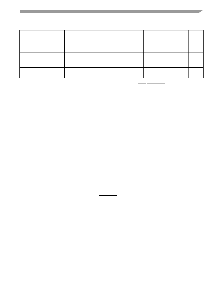
PB[18:31]
P7, P6, P5, P4, P3, P2, P1, R1, R2, R3, R4, R5, R6,
R7
I/0
OVDD
—
PC[0, 1, 4–29]
R8, R9, T9, T6, T5, T4, T1, U1, U2, U3, U4, U7, U8,
U9, U10, V9, V6, V5, V4, V3, V2, V1, W1, W2, W3,
W6, W7, W8
I/0
OVDD
—
PD[7, 14–25, 29–31]
Y4, AA2, AA1, AB1, AB2, AB3, AB5, AB6, AC7, AC4,
AC3, AC2, AC1, AD6, AE3, AE2
I/0
OVDD
—
Notes:
1. All multiplexed signals are listed only once and do not re-occur. For example, LCS5/DMA_REQ2 is listed only once in the
Local Bus Controller Interface section, and is not mentioned in the DMA section even though the pin also functions as
DMA_REQ2.
2. Recommend a weak pull-up resistor (2–10 k
Ω) be placed on this pin to OVDD.
3. TEST_SEL0 must be pulled-high, TEST_SEL1 must be tied to ground.
4. This pin is an open drain signal.
5. This pin is a reset configuration pin. It has a weak internal pull-up P-FET which is enabled only when the MPC8555E is in
the reset state. This pull-up is designed such that it can be overpowered by an external 4.7-k
Ω pull-down resistor. If an
external device connected to this pin might pull it down during reset, then a pull-up or active driver is needed if the signal is
intended to be high during reset.
6. Treat these pins as no connects (NC) unless using debug address functionality.
7. The value of LA[28:31] during reset sets the CCB clock to SYSCLK PLL ratio. These pins require 4.7-k
Ω pull-up or
pull-down resistors. See Section 15.2, “Platform/System PLL Ratio.”
8. The value of LALE and LGPL2 at reset set the e500 core clock to CCB Clock PLL ratio. These pins require 4.7-k
Ω pull-up
or pull-down resistors. See the Section 15.3, “e500 Core PLL Ratio.”
9. Functionally, this pin is an output, but structurally it is an I/O because it either samples configuration input during reset or
because it has other manufacturing test functions. This pin therefore is described as an I/O for boundary scan.
10. This pin functionally requires a pull-up resistor, but during reset it is a configuration input that controls 32- vs. 64-bit PCI
operation. Therefore, it must be actively driven low during reset by reset logic if the device is to be configured to be a 64-bit
PCI device. Refer to the
PCI Specification.
11. This output is actively driven during reset rather than being three-stated during reset.
12. These JTAG pins have weak internal pull-up P-FETs that are always enabled.
13. These pins are connected to the VDD/GND planes internally and may be used by the core power supply to improve tracking
and regulation.
14. Internal thermally sensitive resistor.
15. No connections should be made to these pins.
16. These pins are not connected for any functional use.
17. PCI specifications recommend that a weak pull-up resistor (2–10 k
Ω) be placed on the higher order pins to OVDD when
using 64-bit buffer mode (pins PCI_AD[63:32] and PCI2_C_BE[7:4]).
18. If this pin is connected to a device that pulls down during reset, an external pull-up is required to that is strong enough to
pull this signal to a logic 1 during reset.
19. Recommend a pull-up resistor (~1 k
Ω) be placed on this pin to OVDD.
20. These are test signals for factory use only and must be pulled up (100
Ω το 1kΩ) to OVDD for normal machine operation.
21. If this signal is used as both an input and an output, a weak pull-up (~
10kΩ) is required on this pin.
22. MSYNC_IN and MSYNC_OUT should be connected together for proper operation.
Table 43. MPC8555E Pinout Listing (continued)
Signal
Package Pin Number
Pin Type
Power
Supply
Notes
相关PDF资料 |
PDF描述 |
|---|---|
| IDT70V3379S4BF | IC SRAM 576KBIT 4NS 208FBGA |
| KMPC8555VTALF | IC MPU POWERQUICC III 783-FCPBGA |
| XCS20XL-5TQ144C | IC FPGA 3.3V C-TEMP HP 144TQFP |
| 65801-053LF | CLINCHER RECEPTACLE ASSY GOLD |
| IDT70V3379S4BCG | IC SRAM 576KBIT 4NS 256BGA |
相关代理商/技术参数 |
参数描述 |
|---|---|
| KMPC8555VTAQF | 功能描述:IC MPU POWERQUICC III 783-FCPBGA RoHS:是 类别:集成电路 (IC) >> 嵌入式 - 微处理器 系列:MPC85xx 标准包装:2 系列:MPC8xx 处理器类型:32-位 MPC8xx PowerQUICC 特点:- 速度:133MHz 电压:3.3V 安装类型:表面贴装 封装/外壳:357-BBGA 供应商设备封装:357-PBGA(25x25) 包装:托盘 |
| KMPC855TCVR50D4 | 功能描述:微处理器 - MPU POWER QUICC-NO LEAD RoHS:否 制造商:Atmel 处理器系列:SAMA5D31 核心:ARM Cortex A5 数据总线宽度:32 bit 最大时钟频率:536 MHz 程序存储器大小:32 KB 数据 RAM 大小:128 KB 接口类型:CAN, Ethernet, LIN, SPI,TWI, UART, USB 工作电源电压:1.8 V to 3.3 V 最大工作温度:+ 85 C 安装风格:SMD/SMT 封装 / 箱体:FBGA-324 |
| KMPC855TCVR66D4 | 功能描述:微处理器 - MPU POWER QUICC-NO LEAD RoHS:否 制造商:Atmel 处理器系列:SAMA5D31 核心:ARM Cortex A5 数据总线宽度:32 bit 最大时钟频率:536 MHz 程序存储器大小:32 KB 数据 RAM 大小:128 KB 接口类型:CAN, Ethernet, LIN, SPI,TWI, UART, USB 工作电源电压:1.8 V to 3.3 V 最大工作温度:+ 85 C 安装风格:SMD/SMT 封装 / 箱体:FBGA-324 |
| KMPC855TCZQ50D4 | 功能描述:微处理器 - MPU POWER QUICC RoHS:否 制造商:Atmel 处理器系列:SAMA5D31 核心:ARM Cortex A5 数据总线宽度:32 bit 最大时钟频率:536 MHz 程序存储器大小:32 KB 数据 RAM 大小:128 KB 接口类型:CAN, Ethernet, LIN, SPI,TWI, UART, USB 工作电源电压:1.8 V to 3.3 V 最大工作温度:+ 85 C 安装风格:SMD/SMT 封装 / 箱体:FBGA-324 |
| KMPC855TCZQ66D4 | 功能描述:微处理器 - MPU POWER QUICC RoHS:否 制造商:Atmel 处理器系列:SAMA5D31 核心:ARM Cortex A5 数据总线宽度:32 bit 最大时钟频率:536 MHz 程序存储器大小:32 KB 数据 RAM 大小:128 KB 接口类型:CAN, Ethernet, LIN, SPI,TWI, UART, USB 工作电源电压:1.8 V to 3.3 V 最大工作温度:+ 85 C 安装风格:SMD/SMT 封装 / 箱体:FBGA-324 |
发布紧急采购,3分钟左右您将得到回复。