- 您现在的位置:买卖IC网 > PDF目录30734 > LC74950BG (SANYO SEMICONDUCTOR CO LTD) SPECIALTY CONSUMER CIRCUIT, PBGA96 PDF资料下载
参数资料
| 型号: | LC74950BG |
| 厂商: | SANYO SEMICONDUCTOR CO LTD |
| 元件分类: | 消费家电 |
| 英文描述: | SPECIALTY CONSUMER CIRCUIT, PBGA96 |
| 封装: | 6 X 6 MM, FBGA-96 |
| 文件页数: | 13/37页 |
| 文件大小: | 350K |
| 代理商: | LC74950BG |
第1页第2页第3页第4页第5页第6页第7页第8页第9页第10页第11页第12页当前第13页第14页第15页第16页第17页第18页第19页第20页第21页第22页第23页第24页第25页第26页第27页第28页第29页第30页第31页第32页第33页第34页第35页第36页第37页
LC74950BG
No.A1647-20/37
3) Offset adjustment of video output
Registers related to video output offset adjustment
Name
Functions
Sub address
bit width
ASYG
This register adjusts the offset for the Y/G video signal. It is used when the timing between
the video signal and sync signals is off.
The Y/G video signal can be shifted by an amount equivalent to (ASYG + 1) locks.
0x01
3
ASCRR
This register adjusts the offset for the CR/R video signal. It is used when the timing
between the video signal and sync signals is off.
The CR/R video signal can be shifted by an amount equivalent to (ASCRR + 1) clocks.
0x02
3
ASCBB
This register adjusts the offset for the CB/B video signal. It is used when the timing
between the video signal and sync signals is off.
The CB/B video signal can be shifted by an amount equivalent to (ASVBBYG + 1) clocks.
0x02
3
ASVS
This register adjusts the offset for the VSOUT video signal. It is used when the timing
between the video signal and sync signals is off.
The vertical sync signal can be shifted by an amount equivalent to (ASVS + 1) clocks.
0x03
3
ASHS
This register adjusts the offset for the HSOUT. It is used when the timing between the
video signal and sync signals is off.
The horizontal sync signal can be shifted by an amount equivalent to (ASHS + 1) clocks.
0x03
3
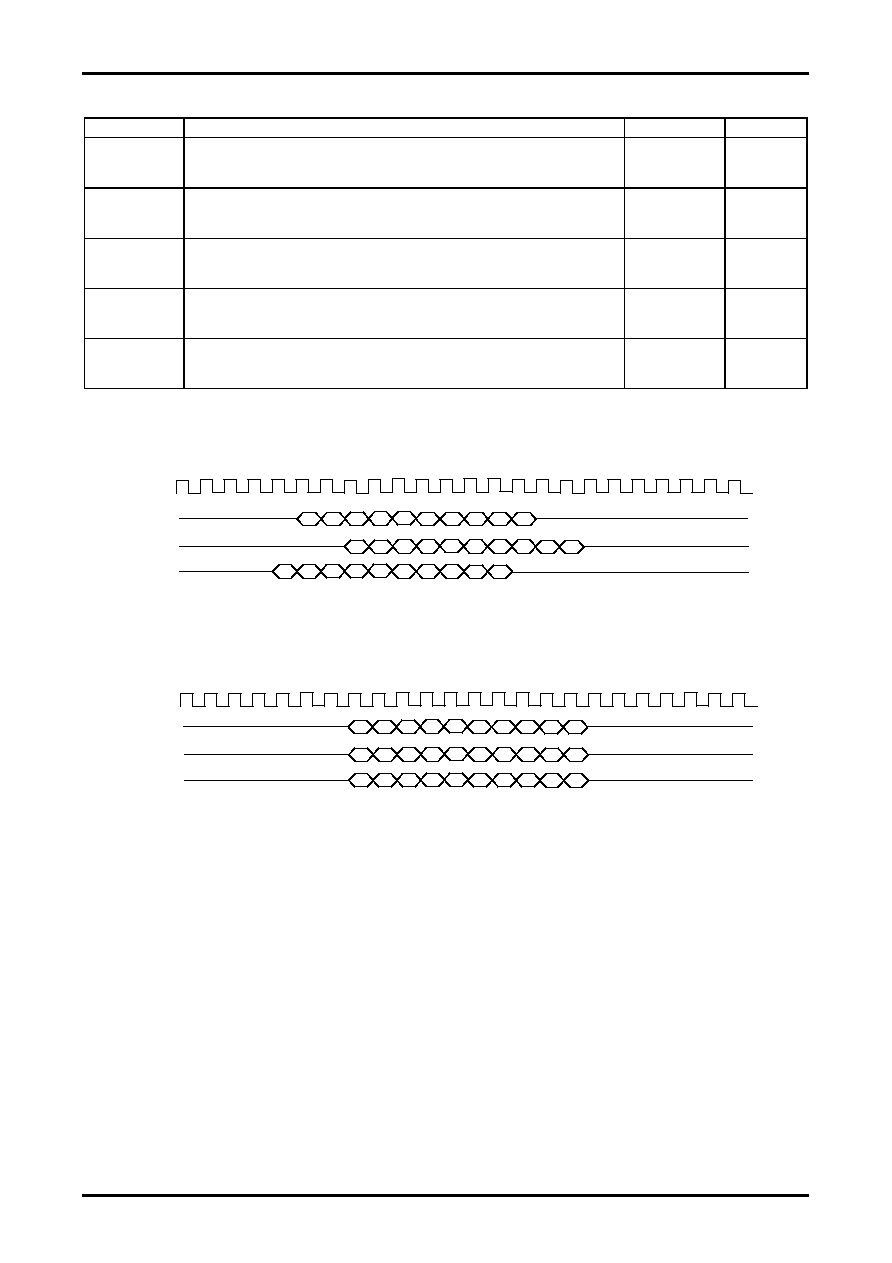
Offset adjustment method
If the following fluctuations are present between the video outputs when ASYG[2:0] = 000b, ASCRR[2:0] = 000b and
ASCBB[2:0] = 000b:
Then, by setting ASYG[2:0] = 010b, ASCRR[2:0] = 000b and ASCBB[2:0] = 011b, the video outputs can be aligned
as shown below. The maximum shift width of the video signals is 8 clocks. If the ASVS[2:0] and ASHS[2:0] registers
are used in line with the video signal shift, the sync signals (VSOUT and HSOUT) can also be shifted in line with the
video signals. (DEOUT is also shifted following HSOUT.)
R0
R1
R2
...
R1439
G0
G1
G2
...
G1439
B0
B1
B2
...
B1439
CLKOUT1
CROUT7-0
YGOUT7-0
CBOUT7-0
R0
R1
R2
...
R1439
G0
G1
G2
...
G1439
B0
B1
B2
...
B1439
CLKOUT1
CROUT7-0
YGOUT7-0
CBOUT7-0
相关PDF资料 |
PDF描述 |
|---|---|
| LC74950BG | SPECIALTY CONSUMER CIRCUIT, PBGA96 |
| LC74980W | SPECIALTY CONSUMER CIRCUIT, PQFP208 |
| LC74981W | SPECIALTY CONSUMER CIRCUIT, PQFP208 |
| LC74982W | SPECIALTY CONSUMER CIRCUIT, PQFP208 |
| LC74986NW-XXXXF | SPECIALTY CONSUMER CIRCUIT, PQFP144 |
相关代理商/技术参数 |
参数描述 |
|---|---|
| LC74950BG-TLM-H | 功能描述:视频模拟/数字化转换器集成电路 RoHS:否 制造商:Texas Instruments 输入信号类型:Differential 转换器数量:1 ADC 输入端数量:4 转换速率:3 Gbps 分辨率:8 bit 结构: 输入电压:3.3 V 接口类型:SPI 信噪比: 电压参考: 电源电压-最大:3.45 V 电源电压-最小:3.15 V 最大功率耗散: 最大工作温度:+ 85 C 最小工作温度:- 40 C 封装 / 箱体:TCSP-48 封装:Reel |
| LC74980W | 制造商:未知厂家 制造商全称:未知厂家 功能描述: |
| LC74981W | 制造商:未知厂家 制造商全称:未知厂家 功能描述: |
| LC74982W | 制造商:SANYO 制造商全称:Sanyo Semicon Device 功能描述:LCD TV Scan Converter IC |
| LC749870W | 制造商:SANYO 制造商全称:Sanyo Semicon Device 功能描述:Silicon gate NTSC/PAL/SECAM Digital Video Decoder |
发布紧急采购,3分钟左右您将得到回复。