- 您现在的位置:买卖IC网 > PDF目录30734 > LC74950BG (SANYO SEMICONDUCTOR CO LTD) SPECIALTY CONSUMER CIRCUIT, PBGA96 PDF资料下载
参数资料
| 型号: | LC74950BG |
| 厂商: | SANYO SEMICONDUCTOR CO LTD |
| 元件分类: | 消费家电 |
| 英文描述: | SPECIALTY CONSUMER CIRCUIT, PBGA96 |
| 封装: | 6 X 6 MM, FBGA-96 |
| 文件页数: | 7/37页 |
| 文件大小: | 350K |
| 代理商: | LC74950BG |
第1页第2页第3页第4页第5页第6页当前第7页第8页第9页第10页第11页第12页第13页第14页第15页第16页第17页第18页第19页第20页第21页第22页第23页第24页第25页第26页第27页第28页第29页第30页第31页第32页第33页第34页第35页第36页第37页
LC74950BG
No.A1647-15/37
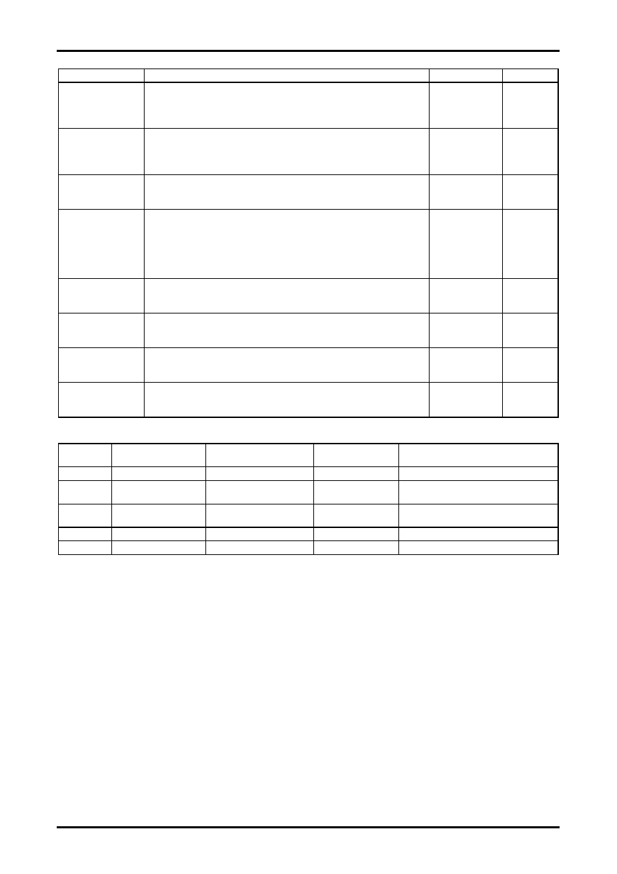
Registers related to the control of clock
Name
Functions
Sub address
bit width
CLKININV
This register controls the inversion of CLKIN when the CLKIN input is used as a
reference clock to PLL.
0: Uses CLKIN in its original form
1: Uses CLKIN in its inverted form
0x00
2
HSINV
This register controls the inversion of HSIN input. The HSIN must be used in its
inverted form when the polarity of HSIN input is negative.
0: Original form (when HSIN is positive)
1: Inverted form (when HSIN is negative)
0x02
1
CLKINDIV
This register sets the frequency division ratio of CLKIN to an arbitrary value
(1/1 to1/64) when the CLKIN is used as a reference clock to PLL.
1/(CLKINDIV[5:0]+1) division
0x40
6
CLKSEL
This register selects the operating mode.
000: (External clock mode (PLL not used)
001: (External clock mode (PLL used)
010: H-lock PLL mode
011: Panel PLL mode <1>
100: Panel PLL mode <2>
0x00
3
CLKADCINV
This register controls the inversion of the ADC sampling clock (CLKADC).
0: Uses CLKADC in its original form
1: Uses CLKADC in its inverted form
0x00
1
CLKOUTINV
This register controls the inversion of the ADC-generated clock. (CLKOUT).
0: Uses CLKOUT in its original form
1: Uses CLKOUT in its inverted form
0x01
1
CLKOUT1INV
This register controls the inversion of CLKOUT (video clock output).
0: Original form
1: Inverted form
0x00
1
CLKOUT2INV
This register controls the inversion of CLKOUT2 (panel clock output).
0: Original form
1: Inverted form
0x00
1
*2 Clock control register (CLKSEL, 00h, bits 2-0) specifications
CLKSEL
(bit2-0)
CLKADC*3
(ADC sampling clock)
FIN
(PLL reference)
CLKOUT2
(Clock output)
Remarks
000
CLKIN/2 (13.5MHz)
L fixed (PLL not used)
CLKIN(27MHz)
External clock mode (PLL not used)
001
FOUT (PLL output)
CLKIN *4
FOUTX2
(PLL output X2)
External clock mode (PLL used)
010
FOUT (PLL output)
HSIN *5
FOUTX2
(PLL output X2)
H-lock PLL mode
011
CLKIN/2
CLKIN *4
FOUT (PLL output)
Panel PLL mode <1>
100
CLKIN
CLKIN *4
FOUT (PLL output)
Panel PLL mode <2>
*3: Register CLKADCINV (00h, bit 3) allows for clock inversion.
*4: Register CLKINDIV (40h, bits 5-0) allows for division of clock frequency (1/1 to 1/64).
*5: Register HSINV (03h, bit 3) allows for HSIN inversion.
相关PDF资料 |
PDF描述 |
|---|---|
| LC74950BG | SPECIALTY CONSUMER CIRCUIT, PBGA96 |
| LC74980W | SPECIALTY CONSUMER CIRCUIT, PQFP208 |
| LC74981W | SPECIALTY CONSUMER CIRCUIT, PQFP208 |
| LC74982W | SPECIALTY CONSUMER CIRCUIT, PQFP208 |
| LC74986NW-XXXXF | SPECIALTY CONSUMER CIRCUIT, PQFP144 |
相关代理商/技术参数 |
参数描述 |
|---|---|
| LC74950BG-TLM-H | 功能描述:视频模拟/数字化转换器集成电路 RoHS:否 制造商:Texas Instruments 输入信号类型:Differential 转换器数量:1 ADC 输入端数量:4 转换速率:3 Gbps 分辨率:8 bit 结构: 输入电压:3.3 V 接口类型:SPI 信噪比: 电压参考: 电源电压-最大:3.45 V 电源电压-最小:3.15 V 最大功率耗散: 最大工作温度:+ 85 C 最小工作温度:- 40 C 封装 / 箱体:TCSP-48 封装:Reel |
| LC74980W | 制造商:未知厂家 制造商全称:未知厂家 功能描述: |
| LC74981W | 制造商:未知厂家 制造商全称:未知厂家 功能描述: |
| LC74982W | 制造商:SANYO 制造商全称:Sanyo Semicon Device 功能描述:LCD TV Scan Converter IC |
| LC749870W | 制造商:SANYO 制造商全称:Sanyo Semicon Device 功能描述:Silicon gate NTSC/PAL/SECAM Digital Video Decoder |
发布紧急采购,3分钟左右您将得到回复。