- 您现在的位置:买卖IC网 > PDF目录15611 > LFM34INTPU1A (Freescale Semiconductor)ADAPTER MPC5534 324-BGA PDF资料下载
参数资料
| 型号: | LFM34INTPU1A |
| 厂商: | Freescale Semiconductor |
| 文件页数: | 15/60页 |
| 文件大小: | 0K |
| 描述: | ADAPTER MPC5534 324-BGA |
| 标准包装: | 1 |
| 模块/板类型: | 适配器板 |
第1页第2页第3页第4页第5页第6页第7页第8页第9页第10页第11页第12页第13页第14页当前第15页第16页第17页第18页第19页第20页第21页第22页第23页第24页第25页第26页第27页第28页第29页第30页第31页第32页第33页第34页第35页第36页第37页第38页第39页第40页第41页第42页第43页第44页第45页第46页第47页第48页第49页第50页第51页第52页第53页第54页第55页第56页第57页第58页第59页第60页
MPC5534 Microcontroller Data Sheet, Rev. 6
Electrical Characteristics
Freescale Semiconductor
22
3.10
eQADC Electrical Characteristics
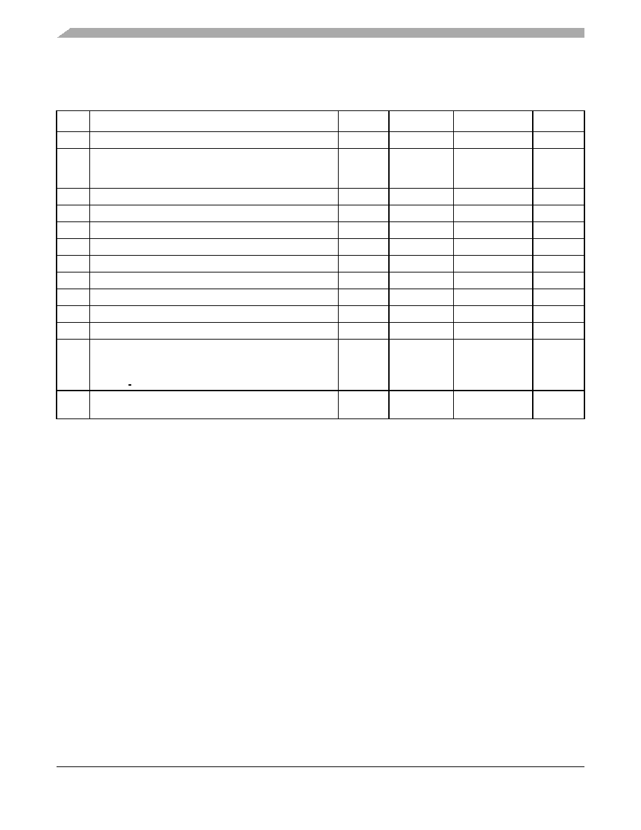
Table 13. eQADC Conversion Specifications (TA = TL to TH)
Spec
Characteristic
Symbol
Minimum
Maximum
Unit
1
ADC clock (ADCLK) frequency 1
1 Conversion characteristics vary with F
ADCLK rate. Reduced conversion accuracy occurs at maximum FADCLK rate. The
maximum value is based on 800 KS/s and the minimum value is based on 20 MHz oscillator clock frequency divided by a
maximum 16 factor.
FADCLK
112
MHz
2
Conversion cycles
Differential
Single ended
CC
13 + 2 (15)
14 + 2 (16)
13 + 128 (141)
14 + 128 (142)
ADCLK
cycles
3
Stop mode recovery time 2
2 Stop mode recovery time begins when the ADC control register enable bits are set until the ADC is ready to perform
conversions.
TSR
10
—
s
4
Resolution 3
3 At V
RH – VRL = 5.12 V, one least significant bit (LSB) = 1.25, mV = one count.
—1.25
—
mV
5
INL: 6 MHz ADC clock
INL6
–4
4
Counts 3
6
INL: 12 MHz ADC clock
INL12
–8
8
Counts
7
DNL: 6 MHz ADC clock
DNL6
–3 4
4 Guaranteed 10-bit mono tonicity.
3 4
Counts
8
DNL: 12 MHz ADC clock
DNL12
–6 4
6 4
Counts
9
Offset error with calibration
OFFWC
–4 5
5 The absolute value of the offset error without calibration
100 counts.
4 5
Counts
10
Full-scale gain error with calibration
GAINWC
–8 6
6 The absolute value of the full scale gain error without calibration
120 counts.
8 6
Counts
11
Disruptive input injection current 7, 8, 9, 10
7 Below disruptive current conditions, the channel being stressed has conversion values of: 0x3FF for analog inputs greater than
VRH, and 0x000 for values less than VRL. This assumes that VRH VDDA and VRL VSSA due to the presence of the sample
amplifier. Other channels are not affected by non-disruptive conditions.
8 Exceeding the limit can cause a conversion error on both stressed and unstressed channels. Transitions within the limit do not
affect device reliability or cause permanent damage.
9 Input must be current limited to the value specified. To determine the value of the required current-limiting resistor, calculate
resistance values using VPOSCLAMP = VDDA + 0.5 V and VNEGCLAMP = – 0.3 V, then use the larger of the calculated values.
10 This condition applies to two adjacent pads on the internal pad.
IINJ
–1
1
mA
12
Incremental error due to injection current. All channels are
10 k
< Rs <100 k
Channel under test has Rs = 10 k
,
IINJ = IINJMAX, IINJMIN
EINJ
–4
4
Counts
13
Total unadjusted error (TUE) for single ended conversions
with calibration 11, 12, 13, 14, 15
11 The TUE specification is always less than the sum of the INL, DNL, offset, and gain errors due to canceling errors.
12 TUE does not apply to differential conversions.
13 Measured at 6 MHz ADC clock. TUE with a 12 MHz ADC clock is: –16 counts < TUE < 16 counts.
14 TUE includes all internal device errors such as internal reference variation (75% Ref, 25% Ref).
15 Depending on the input impedance, the analog input leakage current (Table 9. DC Electrical Specifications, spec 35a) can
affect the actual TUE measured on analog channels AN[12], AN[13], AN[14], AN[15].
TUE
–4
4
Counts
相关PDF资料 |
PDF描述 |
|---|---|
| EEM28DTKT-S288 | CONN EDGECARD 56POS .156 EXTEND |
| ADM6318CY46ARJZ-R7 | IC SUPERVISOR W/RESET SOT23-5 |
| PCG0J471MCL1GS | CAP ALUM 470UF 6.3V 20% SMD |
| MAX6442KAOSTD3+T | IC BATTERY MON DUAL SOT23-8 |
| VI-BW3-EY-F2 | CONVERTER MOD DC/DC 24V 50W |
相关代理商/技术参数 |
参数描述 |
|---|---|
| LFM-39A | 制造商:Leader 功能描述: |
| LFM53INTPU1A | 功能描述:IC 与器件插座 MPC5553 324-PIN BGA TO P RoHS:否 制造商:Molex 产品:LGA Sockets 节距:1.02 mm 排数: 位置/触点数量:2011 触点电镀:Gold 安装风格:SMD/SMT 端接类型:Solder 插座/封装类型:LGA 2011 工作温度范围:- 40 C to + 100 C |
| LFM53INTPWA | 功能描述:IC 与器件插座 MPC5553 416-PIN BGA TO P RoHS:否 制造商:Molex 产品:LGA Sockets 节距:1.02 mm 排数: 位置/触点数量:2011 触点电镀:Gold 安装风格:SMD/SMT 端接类型:Solder 插座/封装类型:LGA 2011 工作温度范围:- 40 C to + 100 C |
| LFM54INTPWA | 功能描述:插座和适配器 PB-FREE MPC5554 BGA TO P RoHS:否 制造商:Silicon Labs 产品:Adapter 用于:EM35x |
| LFM65INTPU1A | 功能描述:插座和适配器 PBSN MPC5565 324 BGA TO RoHS:否 制造商:Silicon Labs 产品:Adapter 用于:EM35x |
发布紧急采购,3分钟左右您将得到回复。