- 您现在的位置:买卖IC网 > PDF目录20330 > LM5051MAX/NOPB (National Semiconductor)IC ORING FET CTRLR 8SOIC PDF资料下载
参数资料
| 型号: | LM5051MAX/NOPB |
| 厂商: | National Semiconductor |
| 文件页数: | 11/23页 |
| 文件大小: | 0K |
| 描述: | IC ORING FET CTRLR 8SOIC |
| 标准包装: | 2,500 |
| 应用: | 冗余电源 |
| FET 型: | N 沟道 |
| 输出数: | 1 |
| 内部开关: | 无 |
| 电源电压: | 36 V ~ 100 V |
| 电流 - 电源: | 400µA |
| 工作温度: | -40°C ~ 125°C |
| 安装类型: | 表面贴装 |
| 封装/外壳: | 8-SOIC(0.154",3.90mm 宽) |
| 供应商设备封装: | 8-SOICN |
| 包装: | 带卷 (TR) |
�� ����
����
����SNVS702D� –� OCTOBER� 2011� –� REVISED� MARCH� 2013�
�APPLICATION� INFORMATION�
�FUNCTIONAL� DESCRIPTION�
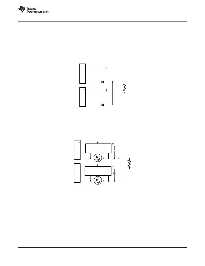
�Systems� that� require� high� availability� often� use� multiple,� parallel-connected� redundant� power� supplies� to� improve�
�reliability.� Schottky� OR-ing� diodes� are� typically� used� to� connect� these� redundant� power� supplies� to� a� common�
�point� at� the� load.� The� disadvantage� of� using� OR-ing� diodes� is� the� forward� voltage� drop,� which� reduces� the�
�available� voltage,� and� the� associated� power� losses� as� load� currents� increase.� Using� an� N-channel� MOSFET� to�
�replace� the� OR-ing� diode� requires� a� small� increase� in� the� level� of� complexity,� but� reduces,� or� eliminates,� the�
�need� for� diode� heat� sinks� or� large� thermal� copper� area� in� circuit� board� layouts� for� high� power� applications.�
�PS1�
�R� LOAD�
�PS2�
�Figure� 26.� Traditional� OR-ing� with� Diodes�
�The� LM5051� is� a� negative� voltage� (i.e.� low-side)� OR-ing� controller� that� will� drive� an� external� N-channel� MOSFET�
�to� replace� an� OR-ing� diode.� The� voltage� across� the� MOSFET� source� and� drain� pins� is� monitored� by� the� LM5051�
�at� the� IN� and� OUT� pins,� while� the� GATE� pin� drives� the� MOSFET� to� control� its� operation� based� on� the� monitored�
�source-drain� voltage.� The� resulting� behavior� is� that� of� an� ideal� rectifier� with� source� and� drain� pins� of� the�
�MOSFET� acting� as� the� anode� and� cathode� pins� of� a� diode� respectively.�
�LINE�
�LM5051�
�VCC�
�PS1�
�PS2�
�INN�
�INN�
�GATE� INP/VSS�
�LINE�
�VCC�
�LM5051�
�GATE� INP/VSS�
�R� LOAD�
�Figure� 27.� OR-ing� with� MOSFETs�
�INP/VSS� PINS�
�The� INP� input� is� internally� connected� to� the� both� device� pin� 5� and� 7.� Typical� applications� will� use� device� pin� 7�
�only,� with� a� single� common� connection� to� the� source� connection� of� the� N-Channel� MOSFET� array.�
�If� pins� 5� and� 7� are� both� used,� it� is� recommended� that� the� two� pins� be� externally� connected� together� at� the�
�package,� with� a� single� common� connection� routed� to� the� source� connection� of� the� N-Channel� MOSFET� array.�
�Current� should� not� be� allowed� flow� through� the� internal� connection� between� pin� 5� and� pin� 7.�
�INN� and� GATE� PINS�
�When� power� is� initially� applied,� the� load� current� will� flow� from� source� to� drain� through� the� body� diode� of� the�
�MOSFET.� The� resulting� voltage� across� the� body� diode� will� be� detected� across� the� LM5051� INN� and� INP/VSS�
�pins� which� then� begins� charging� the� MOSFET� gate� through� a� 0.66� mA� (typical)� current� source.�
�Copyright� ?� 2011–2013,� Texas� Instruments� Incorporated�
�Product� Folder� Links:� LM5051�
��11�
�相关PDF资料 |
PDF描述 |
|---|---|
| IR5001STRPBF | IC CTLR/MOSFET UNIV N-CH 8-SOIC |
| V24A3V3C200BF2 | CONVERTER MOD DC/DC 3.3V 200W |
| ECA15DTKN | CONN EDGECARD 30POS DIP .125 SLD |
| R2S-1524 | CONV DC/DC 2W 15VIN 24VOUT |
| VI-J6M-CW-F4 | CONVERTER MOD DC/DC 10V 100W |
相关代理商/技术参数 |
参数描述 |
|---|---|
| LM5056 | 制造商:TI 制造商全称:Texas Instruments 功能描述:High-Voltage System Power Management Device with PMBusa?¢ |
| LM5056A | 制造商:TI 制造商全称:Texas Instruments 功能描述:High-Voltage System Power Management Device with PMBusa?¢ |
| LM5056APMH/NOPB | 功能描述:PMIC 解决方案 Hi Vtg System Pwr Mgmt IC RoHS:否 制造商:Texas Instruments 安装风格:SMD/SMT 封装 / 箱体:QFN-24 封装:Reel |
| LM5056APMHE/NOPB | 功能描述:PMIC 解决方案 Hi Vtg System Pwr Mgmt IC RoHS:否 制造商:Texas Instruments 安装风格:SMD/SMT 封装 / 箱体:QFN-24 封装:Reel |
| LM5056APMHENOPB | 制造商:Texas Instruments 功能描述:LM5056APMHENOPB |
发布紧急采购,3分钟左右您将得到回复。