- 您现在的位置:买卖IC网 > PDF目录20330 > LM5051MAX/NOPB (National Semiconductor)IC ORING FET CTRLR 8SOIC PDF资料下载
参数资料
| 型号: | LM5051MAX/NOPB |
| 厂商: | National Semiconductor |
| 文件页数: | 15/23页 |
| 文件大小: | 0K |
| 描述: | IC ORING FET CTRLR 8SOIC |
| 标准包装: | 2,500 |
| 应用: | 冗余电源 |
| FET 型: | N 沟道 |
| 输出数: | 1 |
| 内部开关: | 无 |
| 电源电压: | 36 V ~ 100 V |
| 电流 - 电源: | 400µA |
| 工作温度: | -40°C ~ 125°C |
| 安装类型: | 表面贴装 |
| 封装/外壳: | 8-SOIC(0.154",3.90mm 宽) |
| 供应商设备封装: | 8-SOICN |
| 包装: | 带卷 (TR) |
��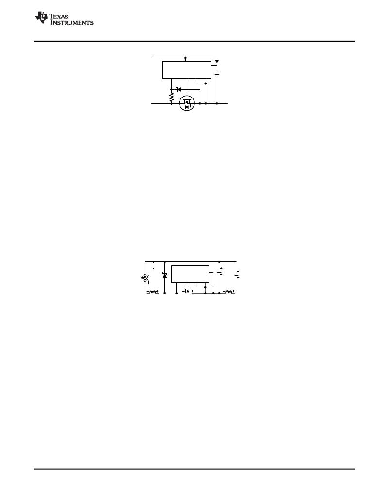 ���
���
���LINE�
�LM5051�
�VCC�
�SNVS702D� –� OCTOBER� 2011� –� REVISED� MARCH� 2013�
�INN�
�GATE� INP/VSS�
�1k�
�Figure� 32.� Protecting� the� INN� Pin�
�SHORT� CIRCUIT� FAILURE� OF� AN� INPUT� SUPPLY�
�An� abrupt� zero� ohm� short� circuit� across� the� input� supply� will� cause� the� highest� possible� reverse� current� to� flow�
�while� the� internal� LM5051� control� circuitry� discharges� the� gate� of� the� MOSFET.� During� this� time,� the� reverse�
�current� is� limited� only� by� the� R� DS(ON)� of� the� MOSFET,� along� with� parasitic� wiring� resistances� and� inductances.�
�Worst� case� instantaneous� reverse� current� would� be� limited� to:�
�I� D(REV)� =� (V� OUT� -� V� IN� )� /� R� DS(ON)�
�(7)�
�The� internal� Reverse� Comparator� will� react,� and� will� start� the� process� of� discharging� the� Gate,� when� the� reverse�
�current� reaches:�
�I� D(REV)� =� V� SD(REV)� /� R� DS(ON)�
�(8)�
�When� the� MOSFET� is� finally� switched� off,� the� energy� stored� in� the� parasitic� wiring� inductances� will� be� transferred�
�to� the� rest� of� the� circuit.�
�LINE�
�Shorted�
�LM5051� VCC�
�INN� GATE� INP/VSS�
�C� OUT�
�C� LOAD�
�Input�
�Parasitic�
�Inductance�
�Parasitic�
�Inductance�
�Figure� 33.� Input� Supply� Fault� Transients�
�MOSFET� SELECTION�
�The� important� MOSFET� electrical� parameters� are� the� maximum� continuous� Drain� current� I� D� ,� the� maximum�
�Source� current� (i.e.� body� diode),� the� maximum� drain-to-source� voltage� V� DS(MAX)� ,� the� gate-to-source� threshold�
�voltage� V� GS(TH)� ,� the� drain-to-source� reverse� breakdown� voltage� V� (BR)DSS� ,� and� the� drain-to-source� On� resistance�
�R� DS(ON)� .�
�The� maximum� continuous� drain� current,� I� D� ,� rating� must� be� exceed� the� maximum� continuous� load� current.� The�
�rating� for� the� maximum� current� through� the� body� diode,� I� S� ,� is� typically� rated� the� same� as,� or� slightly� higher� than�
�the� drain� current,� but� body� diode� current� only� flows� while� the� MOSFET� gate� is� being� charged� to� V� GS(TH)� :�
�Gate� Charge� Time� =� Q� g� /� I� GATE(ON)�
�(9)�
�The� maximum� drain-to-source� voltage,� V� DS(MAX)� ,� must� be� high� enough� to� withstand� the� highest� differential� voltage�
�seen� in� the� application.� This� would� include� any� anticipated� fault� conditions.�
�The� drain-to-source� reverse� breakdown� voltage,� V� (BR)DSS� ,� may� provide� some� transient� protection� to� the� OUT� pin�
�in� low� voltage� applications� by� allowing� conduction� back� to� the� IN� pin� during� positive� transients� at� the� OUT� pin.�
�The� gate-to-source� threshold� voltage,� V� GS(TH)� ,� should� be� compatible� with� the� LM5051� gate� drive� capabilities.�
�Logic� level� MOSFETs� are� recommended,� but� sub-Logic� level� MOSFETs� can� also� be� used.�
�Copyright� ?� 2011–2013,� Texas� Instruments� Incorporated�
�Product� Folder� Links:� LM5051�
��15�
�相关PDF资料 |
PDF描述 |
|---|---|
| IR5001STRPBF | IC CTLR/MOSFET UNIV N-CH 8-SOIC |
| V24A3V3C200BF2 | CONVERTER MOD DC/DC 3.3V 200W |
| ECA15DTKN | CONN EDGECARD 30POS DIP .125 SLD |
| R2S-1524 | CONV DC/DC 2W 15VIN 24VOUT |
| VI-J6M-CW-F4 | CONVERTER MOD DC/DC 10V 100W |
相关代理商/技术参数 |
参数描述 |
|---|---|
| LM5056 | 制造商:TI 制造商全称:Texas Instruments 功能描述:High-Voltage System Power Management Device with PMBusa?¢ |
| LM5056A | 制造商:TI 制造商全称:Texas Instruments 功能描述:High-Voltage System Power Management Device with PMBusa?¢ |
| LM5056APMH/NOPB | 功能描述:PMIC 解决方案 Hi Vtg System Pwr Mgmt IC RoHS:否 制造商:Texas Instruments 安装风格:SMD/SMT 封装 / 箱体:QFN-24 封装:Reel |
| LM5056APMHE/NOPB | 功能描述:PMIC 解决方案 Hi Vtg System Pwr Mgmt IC RoHS:否 制造商:Texas Instruments 安装风格:SMD/SMT 封装 / 箱体:QFN-24 封装:Reel |
| LM5056APMHENOPB | 制造商:Texas Instruments 功能描述:LM5056APMHENOPB |
发布紧急采购,3分钟左右您将得到回复。