- 您现在的位置:买卖IC网 > PDF目录15274 > LTC1149CS-5#PBF (Linear Technology)IC REG CTRLR BUCK PWM CM 16-SOIC PDF资料下载
参数资料
| 型号: | LTC1149CS-5#PBF |
| 厂商: | Linear Technology |
| 文件页数: | 11/20页 |
| 文件大小: | 0K |
| 描述: | IC REG CTRLR BUCK PWM CM 16-SOIC |
| 标准包装: | 50 |
| PWM 型: | 电流模式 |
| 输出数: | 1 |
| 频率 - 最大: | 250kHz |
| 占空比: | 100% |
| 电源电压: | 最高 48V |
| 降压: | 是 |
| 升压: | 无 |
| 回扫: | 无 |
| 反相: | 无 |
| 倍增器: | 无 |
| 除法器: | 无 |
| Cuk: | 无 |
| 隔离: | 无 |
| 工作温度: | 0°C ~ 70°C |
| 封装/外壳: | 16-SOIC(0.154",3.90mm 宽) |
| 包装: | 管件 |
�� �
�
�LTC1149�
�LTC1149-3.3/LTC1149-5�
�APPLICATIO� S� I� FOR� ATIO�
�output� ripple� at� low� frequencies� will� be� large� enough� to� trip�
�the� voltage� comparator.� This� causes� the� Burst� Mode�
�operation� to� be� activated� when� the� LTC1149� series� would�
�normally� be� in� continuous� operation.� The� effect� is� most�
�pronounced� with� low� values� of� R� SENSE� and� can� be�
�improved� by� operating� at� higher� frequencies� with� lower�
�values� of� L.� The� output� remains� in� regulation� at� all� times.�
�Checking� Transient� Response�
�Switching� regulators� take� several� cycles� to� respond� to� a�
�step� in� DC� (resistive)� load� current.� When� a� load� step�
�occurs,� V� OUT� shifts� by� an� amount� equal� to� (� ?� I� LOAD� )(ESR),�
�where� ESR� is� the� effective� series� resistance� of� C� OUT� .�
�?� I� LOAD� also� begins� to� charge� or� discharge� C� OUT� until� the�
�1000�
�L� =� 50� μ� H�
�R� SENSE� =� 0.02� ?�
�regulator� loop� adapts� to� the� current� change� and� returns�
�V� OUT� to� its� steady� state� value.� During� this� recovery� time�
�V� OUT� can� be� monitored� for� overshoot� or� ringing� which�
�would� indicate� a� stability� problem.� The� Pin� 7� external�
�components� shown� in� the� Figure� 1� circuit� will� prove�
�adequate� compensation� for� most� applications.�
�A� second,� more� severe� transient� is� caused� by� switching� in�
�loads� with� large� (>1� μ� F)� supply� bypass� capacitors.� The�
�discharged� bypass� capacitors� are� effectively� put� in� parallel�
�with� C� OUT� ,� causing� a� rapid� drop� in� V� OUT� .� No� regulator� can�
�deliver� enough� current� to� prevent� this� problem� if� the� load�
�switch� resistance� is� low� and� it� is� driven� quickly.� The� only�
�solution� is� to� limit� the� rise� time� of� the� switch� drive� so� that�
�the� load� rise� time� is� limited� to� approximately� (25)(C� LOAD� ).�
�Thus� a� 10� μ� F� capacitor� would� require� a� 250� μ� s� rise� time,�
�limiting� the� charging� current� to� about� 200mA.�
�800�
�LTC1149� Adjustable� Applications�
�600�
�L� =� 25� μ� H�
�R� SENSE� =� 0.02� ?�
�When� an� output� voltage� other� than� 3.3V� or� 5V� is� required,�
�the� LTC1149� adjustable� version� is� used� with� an� external�
�)� )�
�V� OUT� =� 1.25� 1� +� R2�
�400�
�200�
�0�
�0�
�L� =� 50� μ� H�
�R� SENSE� =� 0.05� ?�
�1� 2�
�3�
�4�
�5�
�resistive� divider� from� V� OUT� to� V� FB� Pin� 10.� The� regulated�
�voltage� is� determined:�
�R1�
�(V� IN� –� V� OUT� )� VOLTAGE� (V)�
�1149� F04�
�In� applications� where� V� OUT� is� greater� than� the� LTC1149�
�Figure� 4.� Minimum� Suggested� C� OUT�
�V� IN�
�internally� regulated� V� CC� voltage,� R� SENSE� must� be� moved� to�
�1N4148�
�0.068� μ� F�
�+�
�1� μ� F�
�0V� =� NORMAL�
�>2V� =� SHUTDOWN�
�CAP�
�V� CC�
�V� CC�
�SHDN2�
�V� IN�
�PGATE�
�PDRIVE�
�NGATE�
�LTC1149�
�V� FB�
�1N4148�
�0.047� μ� F�
�100pF�
�IRF9Z34�
�IRFZ34�
�+�
�150� μ� F�
�50V�
�100� μ� H�
�1N5819�
�R2�
�215k�
�1%�
�R1�
�25k�
�+�
�150� μ� F�
�16V�
�OS-CON�
�V� OUT�
�LOAD�
�(� )�
�V� OUT� =� 1.25� 1� +� R2�
�3300pF�
�1k�
�C� T�
�200pF�
�I� TH�
�C� T�
�GNDS�
�SENSE� +�
�SENSE� –�
�1000pF�
�R1�
�VALUES� SHOWN� FOR� V� OUT� =� 12V�
�1%�
�R� SENSE�
�0.05� ?�
�OUTPUT�
�GROUND�
�CONNECTION�
�1149� F05�
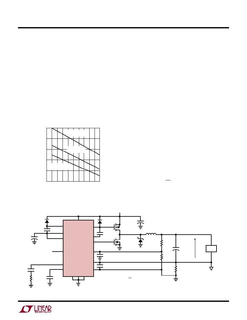
�Figure� 5.� High� Efficiency� Step-Down� Regulator� with� V� OUT� >� V� CC�
�11�
�相关PDF资料 |
PDF描述 |
|---|---|
| LTC1149CS-5 | IC REG CTRLR BUCK PWM CM 16-SOIC |
| EYM22DRST | CONN EDGECARD 44POS DIP .156 SLD |
| EGM22DRST | CONN EDGECARD 44POS DIP .156 SLD |
| LTC3708EUH | IC REG CTRLR BUCK PWM CM 32-QFN |
| LTC3802EUH#PBF | IC REG CTRLR BUCK PWM VM 32-QFN |
相关代理商/技术参数 |
参数描述 |
|---|---|
| LTC1149CSPBF | 制造商:Linear Technology 功能描述:DC-DC Controller Step-Down 48V SOIC16 |
| LTC1150 | 制造商:LINER 制造商全称:Linear Technology 功能描述:15V CHOPPER STABILIZED OPERATIONAL AMPLIFIER WITH INTERNAL CAPACITORS |
| LTC1150_03 | 制造商:LINER 制造商全称:Linear Technology 功能描述:【15V Zero-Drift Operational Amplifier with Internal Capacitors |
| LTC1150C | 制造商:LINER 制造商全称:Linear Technology 功能描述:+-15V Chopper Stabilized Operational Amplifier with Internal Capacitors |
| LTC1150CH | 制造商:未知厂家 制造商全称:未知厂家 功能描述:Chopper-Stabilized Operational Amplifier |
发布紧急采购,3分钟左右您将得到回复。