- 您现在的位置:买卖IC网 > PDF目录15274 > LTC1149CS-5#PBF (Linear Technology)IC REG CTRLR BUCK PWM CM 16-SOIC PDF资料下载
参数资料
| 型号: | LTC1149CS-5#PBF |
| 厂商: | Linear Technology |
| 文件页数: | 15/20页 |
| 文件大小: | 0K |
| 描述: | IC REG CTRLR BUCK PWM CM 16-SOIC |
| 标准包装: | 50 |
| PWM 型: | 电流模式 |
| 输出数: | 1 |
| 频率 - 最大: | 250kHz |
| 占空比: | 100% |
| 电源电压: | 最高 48V |
| 降压: | 是 |
| 升压: | 无 |
| 回扫: | 无 |
| 反相: | 无 |
| 倍增器: | 无 |
| 除法器: | 无 |
| Cuk: | 无 |
| 隔离: | 无 |
| 工作温度: | 0°C ~ 70°C |
| 封装/外壳: | 16-SOIC(0.154",3.90mm 宽) |
| 包装: | 管件 |
�� �
�
�LTC1149�
�LTC1149-3.3/LTC1149-5�
�APPLICATIO� S� I� FOR� ATIO�
�BOLD� LINES� INDICATE� HIGH� CURRENT� PATHS�
�+�
�1N4148�
�0.068� μ� F�
�1N4148�
�P-CHANNEL�
�D1�
�C� IN�
�V� IN�
�1� μ� F�
�+�
�N-CHANNEL�
�–�
�1�
�PGATE�
�CAP�
�16�
�2�
�V� IN�
�SD2�
�15�
�SHUTDOWN�
�0.047� μ� F�
�3�
�4�
�5�
�6�
�V� CC�
�PDRIVE�
�V� CC�
�C� T�
�RGND�
�NGATE�
�PGND�
�SGND�
�14�
�13�
�12�
�11�
�L�
�–�
�C� T�
�3300pF�
�7�
�8�
�I� TH�
�SENSE� –�
�V� FB� /�
�SHDN1�
�SENSE� +�
�10�
�9�
�100pF�
�R1�
�C� OUT�
�V� OUT�
�1k�
�1000pF�
�R2�
�R� SENSE�
�+�
�OUTPUT� DIVIDER� REQUIRED� WITH�
�1149� F08�
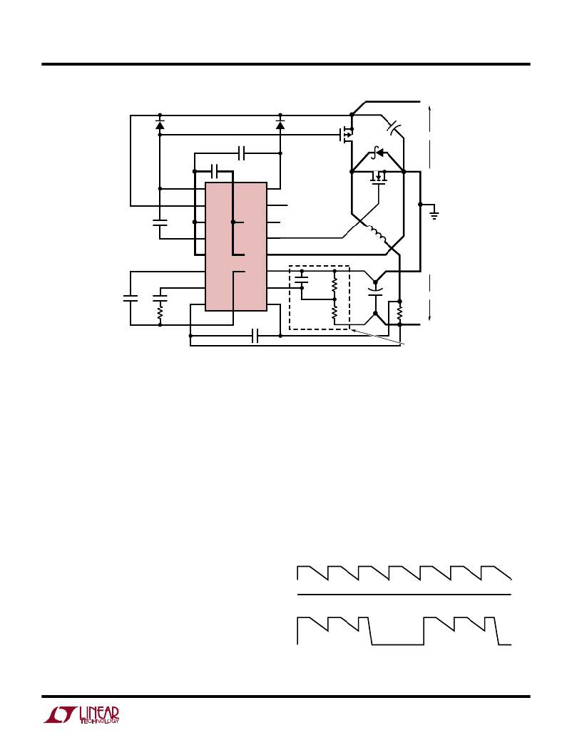
�Figure� 8.� LTC1149� Series� Layout� Diagram� (see� Layout� Checklist)�
�ADJUSTABLE� VERSION� ONLY�
�in� series� with� each� sense� lead� to� help� decouple� Pins� 8�
�and� 9.� However,� when� these� resistors� are� used,� the�
�capacitor� should� be� no� larger� than� 1000pF.�
�4.� Does� the� (+)� plate� of� C� IN� connect� to� the� source� of� the�
�P-channel� MOSFET� as� closely� as� possible?� An� addi-�
�tional� 0.1� μ� F� ceramic� capacitor� between� V� IN� and� power�
�ground� may� be� required� in� some� applications.�
�5.� Is� the� V� CC� decoupling� capacitor� connected� closely�
�between� Pin� 5� of� the� LTC1149� and� power� ground?� This�
�capacitor� carries� the� MOSFET� driver� peak� currents.�
�6.� Is� the� SHDN1� Pin� 10� (fixed� output� versions� only)�
�actively� pulled� to� ground� during� normal� operation?� The�
�SHDN1� pin� is� high� impedance� and� must� not� be� allowed�
�to� float.� In� adjustable� versions,� Pin� 10� is� the� feedback�
�correctly� in� both� continuous� and� Burst� Mode� operation.�
�The� waveform� to� monitor� is� the� voltage� on� the� timing�
�capacitor� Pin� 6.�
�In� continuous� mode� (I� LOAD� >� I� BURST� )� the� voltage� on� Pin� 6�
�should� be� a� sawtooth� with� a� 0.9V� P-P� swing.� This� voltage�
�should� never� dip� below� 2V� as� shown� in� Figure� 9a.�
�When� load� currents� are� low� (I� LOAD� <� I� BURST� )� Burst� Mode�
�operation� should� occur� with� the� C� T� pin� waveform� periodi-�
�cally� falling� to� ground� as� shown� in� Figure� 9b.�
�If� Pin� 6� is� observed� falling� to� ground� at� high� output�
�currents,� it� indicates� poor� decoupling� or� improper� ground-�
�ing.� Refer� to� the� Board� Layout� Checklist.�
�3.3V�
�pin� and� is� very� sensitive� to� pickup� from� the� switch� node.�
�Care� must� be� taken� to� isolate� V� FB� from� possible� capaci-�
�tive� coupling� of� the� inductor� switch� signal.�
�Troubleshooting� Hints�
�Since� efficiency� is� critical� to� LTC1149� series� applications,�
�it� is� very� important� to� verify� that� the� circuit� is� functioning�
�(a)� CONTINUOUS� MODE� OPERATION�
�(b)� Burst� Mode� OPERATION�
�Figure� 9.� C� T� Pin� 6� Waveforms�
�0V�
�3.3V�
�0V�
�1149� F09�
�15�
�相关PDF资料 |
PDF描述 |
|---|---|
| LTC1149CS-5 | IC REG CTRLR BUCK PWM CM 16-SOIC |
| EYM22DRST | CONN EDGECARD 44POS DIP .156 SLD |
| EGM22DRST | CONN EDGECARD 44POS DIP .156 SLD |
| LTC3708EUH | IC REG CTRLR BUCK PWM CM 32-QFN |
| LTC3802EUH#PBF | IC REG CTRLR BUCK PWM VM 32-QFN |
相关代理商/技术参数 |
参数描述 |
|---|---|
| LTC1149CSPBF | 制造商:Linear Technology 功能描述:DC-DC Controller Step-Down 48V SOIC16 |
| LTC1150 | 制造商:LINER 制造商全称:Linear Technology 功能描述:15V CHOPPER STABILIZED OPERATIONAL AMPLIFIER WITH INTERNAL CAPACITORS |
| LTC1150_03 | 制造商:LINER 制造商全称:Linear Technology 功能描述:【15V Zero-Drift Operational Amplifier with Internal Capacitors |
| LTC1150C | 制造商:LINER 制造商全称:Linear Technology 功能描述:+-15V Chopper Stabilized Operational Amplifier with Internal Capacitors |
| LTC1150CH | 制造商:未知厂家 制造商全称:未知厂家 功能描述:Chopper-Stabilized Operational Amplifier |
发布紧急采购,3分钟左右您将得到回复。