- 您现在的位置:买卖IC网 > PDF目录15274 > LTC1149CS-5#PBF (Linear Technology)IC REG CTRLR BUCK PWM CM 16-SOIC PDF资料下载
参数资料
| 型号: | LTC1149CS-5#PBF |
| 厂商: | Linear Technology |
| 文件页数: | 6/20页 |
| 文件大小: | 0K |
| 描述: | IC REG CTRLR BUCK PWM CM 16-SOIC |
| 标准包装: | 50 |
| PWM 型: | 电流模式 |
| 输出数: | 1 |
| 频率 - 最大: | 250kHz |
| 占空比: | 100% |
| 电源电压: | 最高 48V |
| 降压: | 是 |
| 升压: | 无 |
| 回扫: | 无 |
| 反相: | 无 |
| 倍增器: | 无 |
| 除法器: | 无 |
| Cuk: | 无 |
| 隔离: | 无 |
| 工作温度: | 0°C ~ 70°C |
| 封装/外壳: | 16-SOIC(0.154",3.90mm 宽) |
| 包装: | 管件 |
�� �
�
�LTC1149�
�LTC1149-3.3/LTC1149-5�
�OPERATIO�
�(Refer� to� Functional� Diagram)�
�current� is� made� proportional� to� the� output� voltage� (mea-�
�sured� by� Pin� 8)� to� model� the� inductor� current,� which�
�decays� at� a� rate� which� is� also� proportional� to� the� output�
�voltage.� While� the� timing� capacitor� is� discharging,� the�
�NGATE� output� is� high,� turning� on� the� N-channel� MOSFET.�
�When� the� voltage� on� the� timing� capacitor� has� discharged�
�past� V� TH1� ,� comparator� T� trips,� setting� the� flip-flop.� This�
�causes� the� NGATE� output� to� go� low� (turning� off� the�
�N-channel� MOSFET)� and� the� PGATE� output� to� also� go� low�
�(turning� the� P-channel� MOSFET� back� on).� The� cycle� then�
�repeats.�
�As� the� load� current� increases,� the� output� voltage�
�decreases� slightly.� This� causes� the� output� of� the� gain�
�stage� to� increase� the� current� comparator� threshold,� thus�
�tracking� the� load� current.�
�The� sequence� of� events� for� Burst� Mode� operation� is� very�
�similar� to� continuous� operation� with� the� cycle� interrupted�
�by� the� voltage� comparator.� When� the� output� voltage� is� at�
�or� above� the� desired� regulated� value,� the� P-channel� MOSFET�
�is� held� off� by� comparator� V� and� the� timing� capacitor�
�continues� to� discharge� below� V� TH1� .� When� the� timing�
�capacitor� discharges� past� V� TH2� ,� voltage� comparator� S�
�trips,� causing� the� internal� SLEEP� line� to� go� low� and� the�
�N-channel� MOSFET� to� turn� off.�
�The� circuit� now� enters� sleep� mode� with� both� power�
�MOSFETs� turned� off.� In� sleep� mode,� much� of� the� circuitry�
�is� turned� off,� dropping� the� supply� current� from� several�
�milliamperes� (with� the� MOSFETs� switching)� to� 600� μ� A.�
�When� the� output� capacitor� has� discharged� by� the� amount�
�of� hysteresis� in� comparator� V,� the� P-channel� MOSFET� is�
�again� turned� on� and� this� process� repeats.� To� avoid� the�
�operation� of� the� current� loop� interfering� with� Burst� Mode�
�operation,� a� built-in� offset� is� incorporated� in� the� gain�
�stage.� This� prevents� the� current� comparator� threshold�
�from� increasing� until� the� output� voltage� has� dropped�
�below� a� minimum� threshold.�
�To� prevent� both� the� external� MOSFETs� from� ever� being�
�turned� on� at� the� same� time,� feedback� is� incorporated� to�
�sense� the� state� of� the� driver� output� pins.� Before� the� N-gate�
�output� can� go� high,� the� P-drive� output� must� also� be� high.�
�Likewise,� the� P-drive� output� is� prevented� from� going� low�
�when� the� N-gate� output� is� high.�
�Using� constant� off-time� architecture,� the� operating� fre-�
�quency� is� a� function� of� the� input� voltage.� To� minimize� the�
�frequency� variation� as� dropout� is� approached,� the� off-�
�time� controller� increases� the� discharge� current� as� V� IN�
�drops� below� V� OUT� +� 1.5V.� In� dropout� the� P-channel�
�MOSFET� is� turned� on� continuously.�
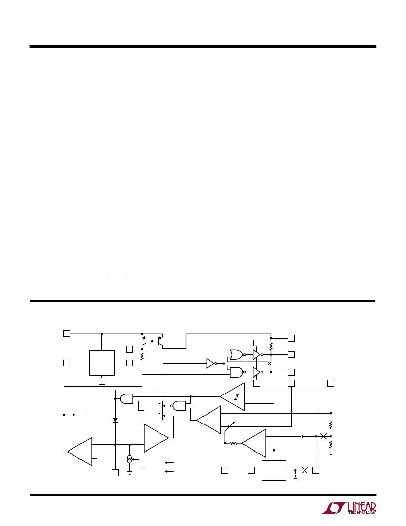
�FU� CTIO� AL� DIAGRA�
�V� IN�
�2�
�Pin� 10� connection� shown� for� LTC1149-3.3� and� LTC1149-5;� changes� create� LTC1149.�
�1� PGATE�
�CAP�
�16�
�5� V� CC�
�500k�
�SHDN2�
�15�
�LOW�
�DROPOUT�
�10V�
�V� CC�
�3�
�500k�
�4� PDRIVE�
�REGULATOR�
�13� NGATE�
�14� RGND�
�12� PGND�
�9� SENSE� +�
�8� SENSE� –�
�V�
�R�
�SLEEP�
�Q�
�S�
�V� TH1�
�C�
�25mV� TO� 150mV�
�V� OS�
�+�
�T�
�13k�
�G�
�100k�
�S�
�–�
�VTH2�
�OFF-TIME�
�V� IN�
�1.25V�
�6�
�C� T�
�CONTROL�
�SENSE� –�
�7�
�I� TH�
�11�
�SGND�
�REFERENCE�
�10�
�SHDN1�
�(V� FB� )�
�1149� FD�
�6�
�相关PDF资料 |
PDF描述 |
|---|---|
| LTC1149CS-5 | IC REG CTRLR BUCK PWM CM 16-SOIC |
| EYM22DRST | CONN EDGECARD 44POS DIP .156 SLD |
| EGM22DRST | CONN EDGECARD 44POS DIP .156 SLD |
| LTC3708EUH | IC REG CTRLR BUCK PWM CM 32-QFN |
| LTC3802EUH#PBF | IC REG CTRLR BUCK PWM VM 32-QFN |
相关代理商/技术参数 |
参数描述 |
|---|---|
| LTC1149CSPBF | 制造商:Linear Technology 功能描述:DC-DC Controller Step-Down 48V SOIC16 |
| LTC1150 | 制造商:LINER 制造商全称:Linear Technology 功能描述:15V CHOPPER STABILIZED OPERATIONAL AMPLIFIER WITH INTERNAL CAPACITORS |
| LTC1150_03 | 制造商:LINER 制造商全称:Linear Technology 功能描述:【15V Zero-Drift Operational Amplifier with Internal Capacitors |
| LTC1150C | 制造商:LINER 制造商全称:Linear Technology 功能描述:+-15V Chopper Stabilized Operational Amplifier with Internal Capacitors |
| LTC1150CH | 制造商:未知厂家 制造商全称:未知厂家 功能描述:Chopper-Stabilized Operational Amplifier |
发布紧急采购,3分钟左右您将得到回复。