- 您现在的位置:买卖IC网 > PDF目录39414 > LTC2215CUP (LINEAR TECHNOLOGY CORP) 1-CH 16-BIT PROPRIETARY METHOD ADC, PARALLEL ACCESS, PQCC64 PDF资料下载
参数资料
| 型号: | LTC2215CUP |
| 厂商: | LINEAR TECHNOLOGY CORP |
| 元件分类: | ADC |
| 英文描述: | 1-CH 16-BIT PROPRIETARY METHOD ADC, PARALLEL ACCESS, PQCC64 |
| 封装: | 9 X 9 MM, PLASTIC, MO-220WNJR-5, QFN-64 |
| 文件页数: | 17/36页 |
| 文件大小: | 1703K |
| 代理商: | LTC2215CUP |
第1页第2页第3页第4页第5页第6页第7页第8页第9页第10页第11页第12页第13页第14页第15页第16页当前第17页第18页第19页第20页第21页第22页第23页第24页第25页第26页第27页第28页第29页第30页第31页第32页第33页第34页第35页第36页
LTC2216/LTC2215
24
22165f
high frequency distortion. A disadvantage of using a
transformer is the loss of low frequency response. Most
small RF transformers have poor performance at frequen-
cies below 1MHz.
Center-tapped transformers provide a convenient means
of DC biasing the secondary; however, they often show
poor balance at high input frequencies, resulting in large
2nd order harmonics.
Figure 4 shows transformer coupling using a transmis-
sion line balun transformer. This type of transformer has
much better high-frequency response and balance than
ux coupled center-tap transformers. Coupling capacitors
are added at the ground and input primary terminals to
allow the secondary terminals to be biased at 1.575V.
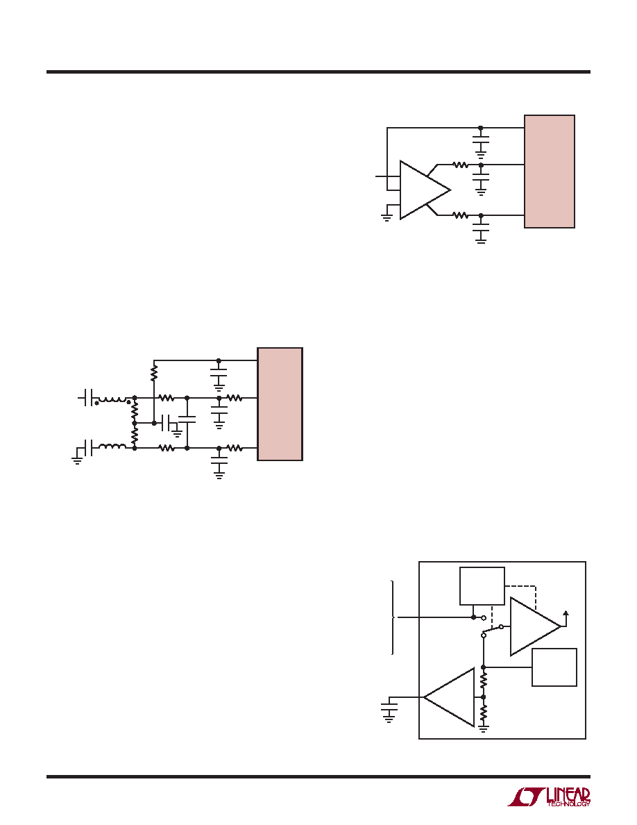
Figure 5. DC Coupled Input with Differential Amplier
0.1μF
AIN
+
AIN
–
4.7pF
2.2μF
4.7pF
VCM
ANALOG
INPUT
0.1μF
5Ω
25Ω
5Ω
25Ω
5Ω
10Ω
T1
1:1
T1 = MA/COM ETC1-1-13
RESISTORS, CAPACITORS
ARE 0402 PACKAGE SIZE
EXCEPT 2.2μF
22165 F04
LTC2216/
LTC2215
Figure 4. Using a Transmission Line Balun Transformer.
Recommended for Input Frequencies from 100MHz to 250MHz
–
+
AIN
+
AIN
–
2.2μF
12pF
VCM
ANALOG
INPUT
22165 F05
CM
AMPLIFIER = LTC6600-20,
LTC1993, ETC.
HIGH SPEED
DIFFERENTIAL
AMPLIFIER
25Ω
LTC2216/
LTC2215
PGA
1.575V
SENSE
VCM
BUFFER
INTERNAL
ADC
REFERENCE
RANGE
SELECT
AND GAIN
CONTROL
2.5V
BANDGAP
REFERENCE
2.2μF
TIE TO VDD TO USE
INTERNAL 2.5V
REFERENCE
OR INPUT AN
EXTERNAL 2.5V
REFERENCE
OR INPUT AN
EXTERNAL 1.25V
REFERENCE
22165 F06
Figure 6. Reference Circuit
Reference Operation
Figure 6 shows the LTC2216/LTC2215 reference circuitry
consisting of a 2.5V bandgap reference, a programmable
gain amplier and control circuit. The LTC2216/LTC2215
has three modes of reference operation: Internal Refer-
ence, 1.25V external reference or 2.5V external reference.
To use the internal reference, tie the SENSE pin to VDD.
To use an external reference, simply apply either a 1.25V
or 2.5V reference voltage to the SENSE input pin. Both
1.25V and 2.5V applied to SENSE will result in a full-scale
range of 2.75VP-P. A 1.575V output, VCM, is provided
for a common mode bias for input drive circuitry. An
external bypass capacitor is required for the VCM output.
This provides a high frequency low impedance path to
ground for internal and external circuitry. This is also
the compensation capacitor for the reference; which will
not be stable without this capacitor. The minimum value
required for stability is 2.2μF.
Direct Coupled Circuits
Figure 5 demonstrates the use of a differential amplier to
convert a single ended input signal into a differential input
signal. The advantage of this method is that it provides
low frequency input response; however, the limited gain
bandwidth of any op amp or closed-loop amplier will de-
grade the ADC SFDR at high input frequencies. Additionally,
wideband op amps or differential ampliers tend to have
high noise. As a result, the SNR will be degraded unless
the noise bandwidth is limited prior to the ADC input.
APPLICATIONS INFORMATION
相关PDF资料 |
PDF描述 |
|---|---|
| LTC2216CUP#TR | 1-CH 16-BIT PROPRIETARY METHOD ADC, PARALLEL ACCESS, PQCC64 |
| LTC2216IUP#TR | 1-CH 16-BIT PROPRIETARY METHOD ADC, PARALLEL ACCESS, PQCC64 |
| LTC2216IUP | 1-CH 16-BIT PROPRIETARY METHOD ADC, PARALLEL ACCESS, PQCC64 |
| LTC2216CUP | 1-CH 16-BIT PROPRIETARY METHOD ADC, PARALLEL ACCESS, PQCC64 |
| LTC2215IUP | 1-CH 16-BIT PROPRIETARY METHOD ADC, PARALLEL ACCESS, PQCC64 |
相关代理商/技术参数 |
参数描述 |
|---|---|
| LTC2215CUP#PBF | 制造商:Linear Technology 功能描述:IC ADC 16BIT 65MSPS 64-QFN |
| LTC2215CUP#TRPBF | 制造商:Linear Technology 功能描述:IC ADC 16BIT 65MSPS 64-QFN |
| LTC2215CUP-PBF | 制造商:LINER 制造商全称:Linear Technology 功能描述:16-Bit, 80Msps/65Msps Low Noise ADC |
| LTC2215CUP-TR | 制造商:LINER 制造商全称:Linear Technology 功能描述:16-Bit, 80Msps/65Msps Low Noise ADC |
| LTC2215CUP-TRPBF | 制造商:LINER 制造商全称:Linear Technology 功能描述:16-Bit, 80Msps/65Msps Low Noise ADC |
发布紧急采购,3分钟左右您将得到回复。