- 您现在的位置:买卖IC网 > PDF目录39414 > LTC2215CUP (LINEAR TECHNOLOGY CORP) 1-CH 16-BIT PROPRIETARY METHOD ADC, PARALLEL ACCESS, PQCC64 PDF资料下载
参数资料
| 型号: | LTC2215CUP |
| 厂商: | LINEAR TECHNOLOGY CORP |
| 元件分类: | ADC |
| 英文描述: | 1-CH 16-BIT PROPRIETARY METHOD ADC, PARALLEL ACCESS, PQCC64 |
| 封装: | 9 X 9 MM, PLASTIC, MO-220WNJR-5, QFN-64 |
| 文件页数: | 20/36页 |
| 文件大小: | 1703K |
| 代理商: | LTC2215CUP |
第1页第2页第3页第4页第5页第6页第7页第8页第9页第10页第11页第12页第13页第14页第15页第16页第17页第18页第19页当前第20页第21页第22页第23页第24页第25页第26页第27页第28页第29页第30页第31页第32页第33页第34页第35页第36页
LTC2216/LTC2215
27
22165f
resistor, even if the signal is not used (such as OF+/OF– or
CLKOUT+/CLKOUT–). To minimize noise the PC board
traces for each LVDS output pair should be routed close
together. To minimize clock skew all LVDS PC board traces
should have about the same length.
In Low Power LVDS Mode 1.75mA is steered between
the differential outputs, resulting in ±175mV at the LVDS
receiver’s 100
Ω termination resistor. The output com-
mon mode voltage is 1.20V, the same as standard LVDS
Mode.
Data Format
The LTC2216/LTC2215 parallel digital output can be
selected for offset binary or 2’s complement format. The
format is selected with the MODE pin. This pin has a four
level logic input, centered at 0, 1/3VDD, 2/3VDD and VDD.
An external resistor divider can be user to set the 1/3VDD
and 2/3VDD logic levels. Table 2 shows the logic states
for the MODE pin.
Table 2. MODE Pin Function
MODE
OUTPUT FORMAT
CLOCK DUTY
CYCLE STABILIZER
0V(GND)
Offset Binary
Off
1/3VDD
Offset Binary
On
2/3VDD
2’s Complement
On
VDD
2’s Complement
Off
22165 F12
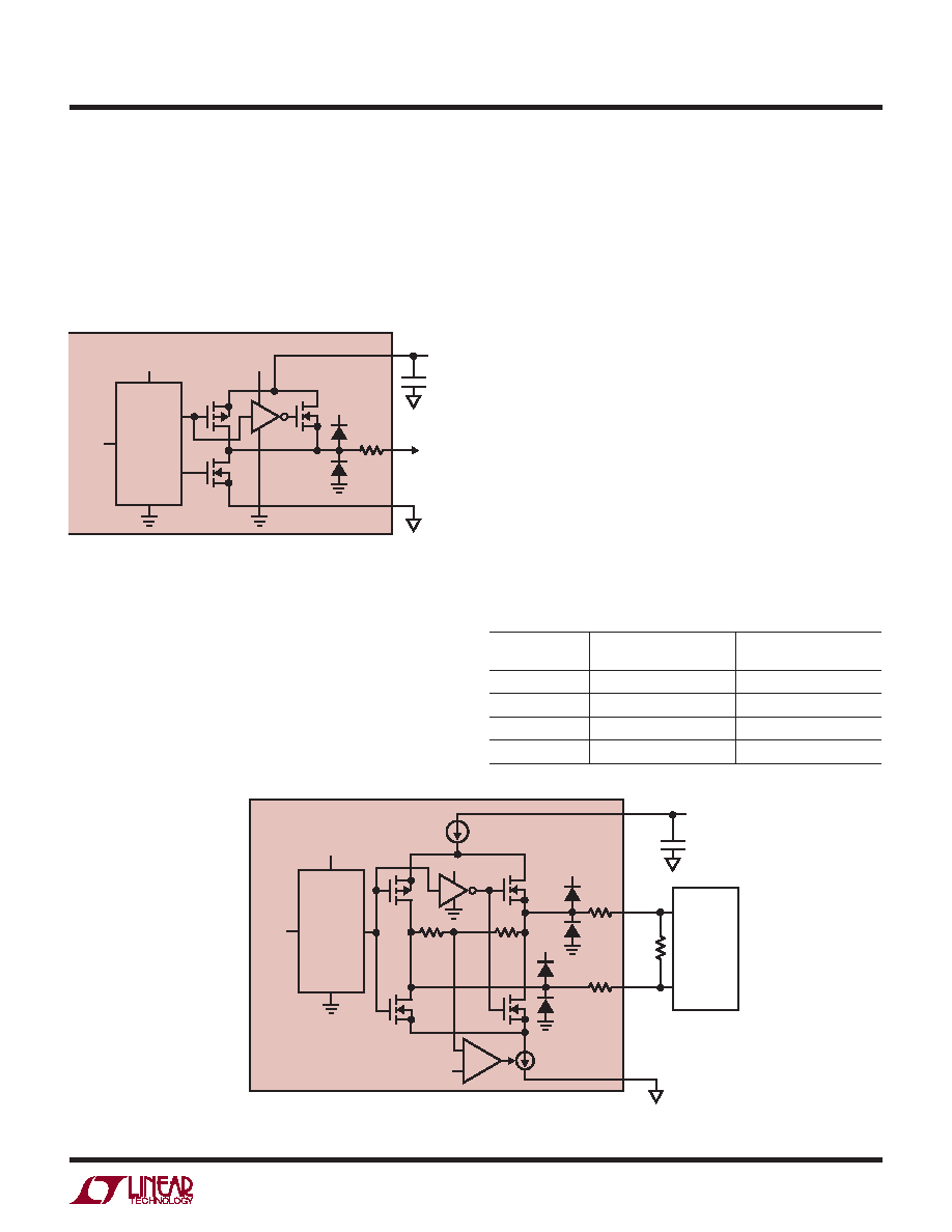
OVDD
VDD
0.1μF
TYPICAL
DATA
OUTPUT
OGND
OVDD
0.5V
TO 3.6V
PREDRIVER
LOGIC
DATA
FROM
LATCH
43Ω
LTC2216/LTC2215
Figure 12. Equivalent Circuit for a Digital Output Buffer
ALVCH16373 CMOS latch. For full speed operation the
capacitive load should be kept under 10pF. A resistor in
series with the output may be used, but is not required
since the ADC has a series resistor of 43
Ω on-chip.
Lower OVDD voltages will also help reduce interference
from the digital outputs.
Digital Output Buffers (LVDS Modes)
Figure 13 shows an equivalent circuit for an LVDS output
pair. A 3.5mA current is steered from OUT+ to OUT– or
vice versa, which creates a ±350mV differential voltage
across the 100
Ω termination resistor at the LVDS receiver.
A feedback loop regulates the common mode output volt-
age to 1.20V. For proper operation each LVDS output pair
must be terminated with an external 100
Ω termination
22165 F13
3.5mA
1.20V
LVDS
RECEIVER
OGND
10k
VDD
0.1μF
OVDD
3.3V
PREDRIVER
LOGIC
DATA
FROM
LATCH
+
–
OVDD
43Ω
100Ω
LTC2216/LTC2215
Figure 13. Equivalent Output Buffer in LVDS Mode
APPLICATIONS INFORMATION
相关PDF资料 |
PDF描述 |
|---|---|
| LTC2216CUP#TR | 1-CH 16-BIT PROPRIETARY METHOD ADC, PARALLEL ACCESS, PQCC64 |
| LTC2216IUP#TR | 1-CH 16-BIT PROPRIETARY METHOD ADC, PARALLEL ACCESS, PQCC64 |
| LTC2216IUP | 1-CH 16-BIT PROPRIETARY METHOD ADC, PARALLEL ACCESS, PQCC64 |
| LTC2216CUP | 1-CH 16-BIT PROPRIETARY METHOD ADC, PARALLEL ACCESS, PQCC64 |
| LTC2215IUP | 1-CH 16-BIT PROPRIETARY METHOD ADC, PARALLEL ACCESS, PQCC64 |
相关代理商/技术参数 |
参数描述 |
|---|---|
| LTC2215CUP#PBF | 制造商:Linear Technology 功能描述:IC ADC 16BIT 65MSPS 64-QFN |
| LTC2215CUP#TRPBF | 制造商:Linear Technology 功能描述:IC ADC 16BIT 65MSPS 64-QFN |
| LTC2215CUP-PBF | 制造商:LINER 制造商全称:Linear Technology 功能描述:16-Bit, 80Msps/65Msps Low Noise ADC |
| LTC2215CUP-TR | 制造商:LINER 制造商全称:Linear Technology 功能描述:16-Bit, 80Msps/65Msps Low Noise ADC |
| LTC2215CUP-TRPBF | 制造商:LINER 制造商全称:Linear Technology 功能描述:16-Bit, 80Msps/65Msps Low Noise ADC |
发布紧急采购,3分钟左右您将得到回复。