- 您现在的位置:买卖IC网 > PDF目录369885 > LXT384BE Telecomm/Datacomm PDF资料下载
参数资料
| 型号: | LXT384BE |
| 元件分类: | 通信、网络模块及开发工具 |
| 英文描述: | Telecomm/Datacomm |
| 中文描述: | 电信/数据通信 |
| 文件页数: | 16/80页 |
| 文件大小: | 1112K |
| 代理商: | LXT384BE |
第1页第2页第3页第4页第5页第6页第7页第8页第9页第10页第11页第12页第13页第14页第15页当前第16页第17页第18页第19页第20页第21页第22页第23页第24页第25页第26页第27页第28页第29页第30页第31页第32页第33页第34页第35页第36页第37页第38页第39页第40页第41页第42页第43页第44页第45页第46页第47页第48页第49页第50页第51页第52页第53页第54页第55页第56页第57页第58页第59页第60页第61页第62页第63页第64页第65页第66页第67页第68页第69页第70页第71页第72页第73页第74页第75页第76页第77页第78页第79页第80页
LXT384
—
Octal T1/E1/J1 Transceiver
16
Datasheet
21
22
23
24
25
26
27
28
G2
H3
H2
J4
J3
J2
J1
K1
LOOP0/D0
LOOP1/D1
LOOP2/D2
LOOP3/D3
LOOP4/D4
LOOP5/D5
LOOP6/D6
LOOP7/D7
DI/O
DI/O
DI/O
DI/O
DI/O
DI/O
DI/O
DI/O
Loopback Mode Select/Parallel Data bus Input &Output.
Host Mode
When a non-multiplexed microprocessor interface is selected, these
pins function as a bi-directional 8-bit data port.
When a multiplexed microprocessor interface is selected, these pins
carry both bi-directional 8-bit data and address inputs A0 -A7.
In serial Mode, D0-7 should be grounded.
Hardware Mode
In hardware mode, the LXT384 works in normal operation if this pin is
left open (unconnected).
The LXT384 enters remote loopback mode, if this pin is Low. In this
mode, data on TPOS and TNEG is ignored and data received on RTIP
and RRING is looped around and retransmitted on TTIP and TRING.
Note: in data recovery mode, the pulse template cannot be guaranteed
while in a remote loopback.
The LXT384 enters analog local loopback mode, if this pin is High. In
this mode, data received on RTIP and RRING is ignored and data
transmitted on TTIP and TRING is internally looped around and routed
back to the receive inputs.
Note:
When these inputs are left open, they stay in a high impedance
state. Therefore, the layout design should not route signals with
fast transitions near the LOOP pins. This practice will minimize
capacitive coupling.
29
L1
TCLK1
DI
Transmit Clock Input.
30
30
31
31
L2
L2
L3
L3
TPOS1
TDATA1
TNEG1
UBS1
DI
DI
DI
DI
Transmit Positive Data Input.
Transmit Data Input.
Transmit Negative Data Input.
Unipolar/Bipolar Select Input.
32
M1
RCLK1
DO
Receive Clock Output.
33
33
34
34
M2
M2
M3
M3
RPOS1
RDATA1
RNEG1
BPV1
DO
DO
DO
DO
Receive Positive Data Output.
Receive Data Output.
Receive Negative Data Output.
Bipolar Violation Detect Output.
35
K3
LOS1
DO
Loss of Signal Output.
36
N1
TCLK0
DI
Transmit Clock Input.
37
37
38
38
N2
N2
N3
N3
TPOS0
TDATA0
TNEG0
UBS0
DI
DI
DI
DI
Transmit Positive Data Input.
Transmit Data Input.
Transmit Negative Data Input.
Unipolar/Bipolar Select Input.
39
P1
RCLK0
DO
Receive Clock Output.
40
40
41
41
P2
P2
P3
P3
RPOS0
RDATA0
RNEG0
BPV0
DO
DO
DO
DO
Receive Positive Data.
Receive Data Output.
Receive Negative Data.
Bipolar Violation Detect.
42
K4
LOS0
DO
Loss of Signal Output.
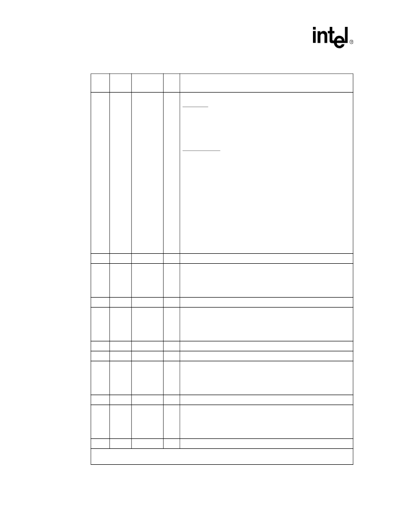
Table 1. LXT384 Pin Description (Sheet 6 of 12)
Pin #
QFP
Ball #
PBGA
Symbol
I/O
1
Description
1. DI: Digital Input; DO: Digital Output; DI/O: Digital Bidirectional Port; AI: Analog Input; AO: Analog Output
S: Power Supply; N.C.: Not Connected.
相关PDF资料 |
PDF描述 |
|---|---|
| LXT384LE | Telecomm/Datacomm |
| LXT386BE | PCM TRANSCEIVER|QUAD|CEPT PCM-30/E-1|CMOS|BGA|160PIN|PLASTIC |
| LXT386LE | PCM TRANSCEIVER|QUAD|CEPT PCM-30/E-1|CMOS|QFP|100PIN|PLASTIC |
| LXT388LE | PCM TRANSCEIVER|DUAL|CEPT PCM-30/E-1|CMOS|QFP|100PIN|PLASTIC |
| LXT400JE | Hermetically Sealed, 3.3V, High Speed, High CMR, Logic Gate Optocoupler |
相关代理商/技术参数 |
参数描述 |
|---|---|
| LXT384LE | 制造商:未知厂家 制造商全称:未知厂家 功能描述:Telecomm/Datacomm |
| LXT386 | 制造商:INTEL 制造商全称:Intel Corporation 功能描述:QUAD T1/E1/J1 Transceiver |
| LXT386BE | 制造商:未知厂家 制造商全称:未知厂家 功能描述:PCM TRANSCEIVER|QUAD|CEPT PCM-30/E-1|CMOS|BGA|160PIN|PLASTIC |
| LXT386LE | 制造商:LEVEL1 功能描述: |
| LXT388LE | 制造商:未知厂家 制造商全称:未知厂家 功能描述:PCM TRANSCEIVER|DUAL|CEPT PCM-30/E-1|CMOS|QFP|100PIN|PLASTIC |
发布紧急采购,3分钟左右您将得到回复。