- 您现在的位置:买卖IC网 > PDF目录369885 > LXT384BE Telecomm/Datacomm PDF资料下载
参数资料
| 型号: | LXT384BE |
| 元件分类: | 通信、网络模块及开发工具 |
| 英文描述: | Telecomm/Datacomm |
| 中文描述: | 电信/数据通信 |
| 文件页数: | 35/80页 |
| 文件大小: | 1112K |
| 代理商: | LXT384BE |
第1页第2页第3页第4页第5页第6页第7页第8页第9页第10页第11页第12页第13页第14页第15页第16页第17页第18页第19页第20页第21页第22页第23页第24页第25页第26页第27页第28页第29页第30页第31页第32页第33页第34页当前第35页第36页第37页第38页第39页第40页第41页第42页第43页第44页第45页第46页第47页第48页第49页第50页第51页第52页第53页第54页第55页第56页第57页第58页第59页第60页第61页第62页第63页第64页第65页第66页第67页第68页第69页第70页第71页第72页第73页第74页第75页第76页第77页第78页第79页第80页
Octal T1/E1/J1 Transceiver
—
LXT384
Datasheet
35
2.11
Interfacing with 5V Logic
The LXT384 can interface directly with 5V TTL family devices. The internal input pads are
tolerant to 5V outputs from TTL and CMOS family devices.
2.12
Parallel Host Interface
The LXT384 incorporates a highly flexible 8-bit parallel microprocessor interface. The interface is
generic and is designed to support both non-multiplexed and multiplexed address/data bus systems
for Motorola and Intel bus topologies. Two pins (MUX and MOT/INTL) select four different
operating modes as shown in
Table 5
.
The interface includes an address bus (A4 - A0) and a data bus (D7 - D0) for non-multiplexed
operation and an 8-bit address/data bus for multiplexed operation. WR, RD, R/W, CS, ALE, DS,
INT and RDY/ACK are used as control signals. A significant enhancement is an internal wait-state
generator that controls an Intel and Motorola compatible handshake output signal (RDY/ACK). In
Motorola mode, ACK Low signals valid information is on the data bus. During a write cycle a Low
signal acknowledges the acceptance of the write data.
In Intel mode, RDY High signals to the controlling processor that the bus cycle can be completed.
While Low the microprocessor must insert wait states. This allows the LXT384 to interface with
wait-state capable microcontrollers, independent of the processor bus speed. To activate this
function a reference clock is required on the MCLK pin.
There is one exception to write cycle timing for Intel non-multiplexed mode: Register 0Ah, the
reset register. Because of timing issues, the RDY line remains high after the first part of the cycle is
done, not signalling write cycle completion with another transition low. Add 2 microseconds of
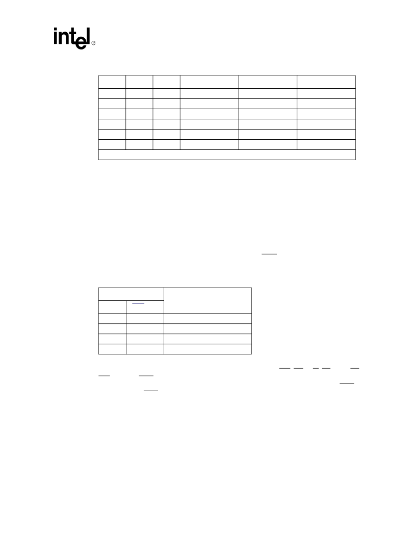
H
Clocked
H
Data Recovery
Pulse Shaping ON
Analog Loopback
H
L
Open
Data Recovery
Power down
No Loopback
H
L
L
Data Recovery
Pulse Shaping OFF
Remote Loopback
H
H
Open
Data Recovery
Pulse Shaping OFF
No Loopback
H
H
L
Data Recovery
Pulse Shaping OFF
Remote Loopback
H
H
H
Data Recovery
Pulse Shaping OFF
Analog Loopback
Table 4. Operation Mode Summary (Continued)
MCLK
TCLK
LOOP
1
Receive Mode
Transmit Mode
Loopback
1. Hardware mode only.
Table 5. Microprocessor Interface Selection
Pin
Operating Mode
MUX
MOT/INTL
Low
Low
Motorola, Non-Multiplexed
Low
High
Intel, Non-Multiplexed
High
Low
Motorola, Multiplexed
High
High
Intel, Multiplexed
相关PDF资料 |
PDF描述 |
|---|---|
| LXT384LE | Telecomm/Datacomm |
| LXT386BE | PCM TRANSCEIVER|QUAD|CEPT PCM-30/E-1|CMOS|BGA|160PIN|PLASTIC |
| LXT386LE | PCM TRANSCEIVER|QUAD|CEPT PCM-30/E-1|CMOS|QFP|100PIN|PLASTIC |
| LXT388LE | PCM TRANSCEIVER|DUAL|CEPT PCM-30/E-1|CMOS|QFP|100PIN|PLASTIC |
| LXT400JE | Hermetically Sealed, 3.3V, High Speed, High CMR, Logic Gate Optocoupler |
相关代理商/技术参数 |
参数描述 |
|---|---|
| LXT384LE | 制造商:未知厂家 制造商全称:未知厂家 功能描述:Telecomm/Datacomm |
| LXT386 | 制造商:INTEL 制造商全称:Intel Corporation 功能描述:QUAD T1/E1/J1 Transceiver |
| LXT386BE | 制造商:未知厂家 制造商全称:未知厂家 功能描述:PCM TRANSCEIVER|QUAD|CEPT PCM-30/E-1|CMOS|BGA|160PIN|PLASTIC |
| LXT386LE | 制造商:LEVEL1 功能描述: |
| LXT388LE | 制造商:未知厂家 制造商全称:未知厂家 功能描述:PCM TRANSCEIVER|DUAL|CEPT PCM-30/E-1|CMOS|QFP|100PIN|PLASTIC |
发布紧急采购,3分钟左右您将得到回复。