- 您现在的位置:买卖IC网 > PDF目录369885 > LXT384BE Telecomm/Datacomm PDF资料下载
参数资料
| 型号: | LXT384BE |
| 元件分类: | 通信、网络模块及开发工具 |
| 英文描述: | Telecomm/Datacomm |
| 中文描述: | 电信/数据通信 |
| 文件页数: | 20/80页 |
| 文件大小: | 1112K |
| 代理商: | LXT384BE |
第1页第2页第3页第4页第5页第6页第7页第8页第9页第10页第11页第12页第13页第14页第15页第16页第17页第18页第19页当前第20页第21页第22页第23页第24页第25页第26页第27页第28页第29页第30页第31页第32页第33页第34页第35页第36页第37页第38页第39页第40页第41页第42页第43页第44页第45页第46页第47页第48页第49页第50页第51页第52页第53页第54页第55页第56页第57页第58页第59页第60页第61页第62页第63页第64页第65页第66页第67页第68页第69页第70页第71页第72页第73页第74页第75页第76页第77页第78页第79页第80页
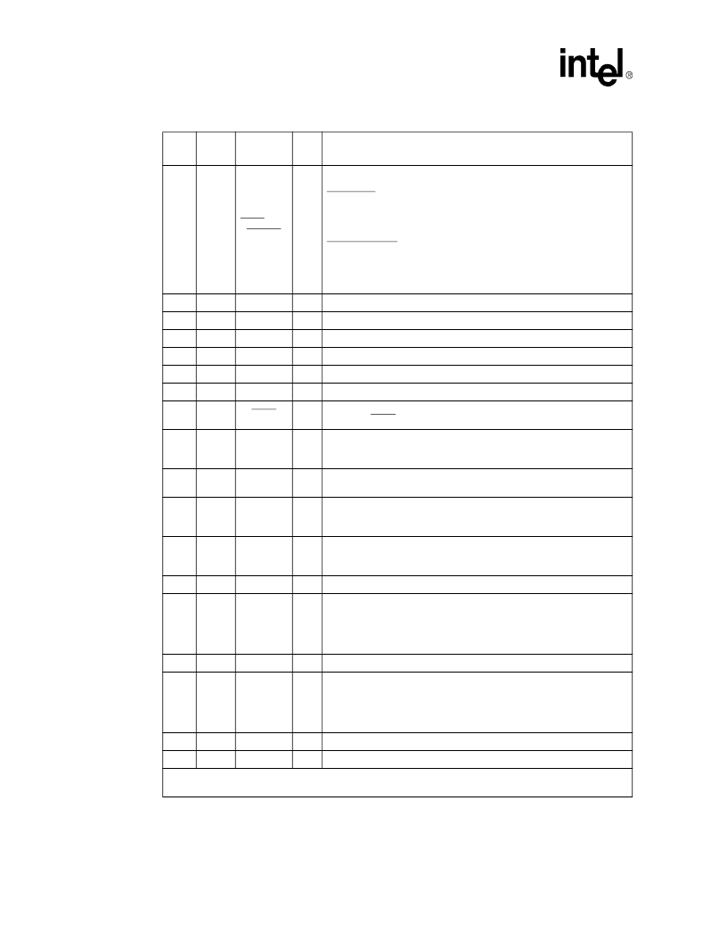
LXT384
—
Octal T1/E1/J1 Transceiver
20
Datasheet
88
H12
MOT/INTL/
CODEN
DI
Motorola/Intel/Codec Enable Select Input.
Host Mode:
When Low, the host interface is configured for Motorola
microcontrollers. When High, the host interface is configured for Intel
microcontrollers.
Hardware Mode:
Determines the line encode/decode selection when in unipolar mode.
When Low, B8ZS/HDB3 encoders/decoders are enabled for T1/E1
respectively. When High, enables AMI encoder/decoder (transparent
mode).
89
H11
GND1
S
Ground (Core).
90
H14
VCC1
S
Power (Core).
91
G11
GNDIO1
S
Ground (I/O).
92
G14
VCCIO1
S
Power (I/O).
93
G13
AT2
AO
JTAG Analog Output Test Port 2.
94
H13
AT1
AI
JTAG Analog Input Test Port 1.
95
G12
TRST
JTAG Controller Reset Input.
Input is used to reset the JTAG
controller. TRST is pulled up internally and may be left disconnected.
96
F11
TMS
DI
JTAG Test Mode Select Input.
Used to control the test logic state
machine. Sampled on rising edge of TCK. TMS is pulled up internally
and may be left disconnected.
97
F14
TCK
DI
JTAG Clock Input.
Clock input for JTAG. Connect to GND when not
used.
98
F13
TDO
DO
JTAG Data Output.
Test Data Output for JTAG. Used for reading all
serial configuration and test data from internal test logic. Updated on
falling edge of TCK.
99
F12
TDI
DI
JTAG Data Input.
Test Data input for JTAG. Used for loading serial
instructions and data into internal test logic. Sampled on rising edge of
TCK. TDI is pulled up internally and may be left disconnected.
100
D14
TCLK5
DI
Transmit Clock Input.
101
101
102
102
D13
D13
D12
D12
TPOS5
TDATA5
TNEG5
UBS5
DI
DI
DI
DI
Transmit Positive Data Input.
Transmit Data Input.
Transmit Negative Data Input.
Unipolar/Bipolar Select Input.
103
C14
RCLK5
DO
Receive Clock Output.
104
104
105
105
C13
C13
C12
C12
RPOS5
RDATA5
RNEG5
BPV5
DO
DO
DO
DO
Receive Positive Data Output.
Receive Data Output.
Receive Negative Data Output.
Bipolar Violation Detect Output.
106
E12
LOS5
DO
Loss of Signal Output.
107
B14
TCLK4
DI
Transmit Clock Input.
Table 1. LXT384 Pin Description (Sheet 10 of 12)
Pin #
QFP
Ball #
PBGA
Symbol
I/O
1
Description
1. DI: Digital Input; DO: Digital Output; DI/O: Digital Bidirectional Port; AI: Analog Input; AO: Analog Output
S: Power Supply; N.C.: Not Connected.
相关PDF资料 |
PDF描述 |
|---|---|
| LXT384LE | Telecomm/Datacomm |
| LXT386BE | PCM TRANSCEIVER|QUAD|CEPT PCM-30/E-1|CMOS|BGA|160PIN|PLASTIC |
| LXT386LE | PCM TRANSCEIVER|QUAD|CEPT PCM-30/E-1|CMOS|QFP|100PIN|PLASTIC |
| LXT388LE | PCM TRANSCEIVER|DUAL|CEPT PCM-30/E-1|CMOS|QFP|100PIN|PLASTIC |
| LXT400JE | Hermetically Sealed, 3.3V, High Speed, High CMR, Logic Gate Optocoupler |
相关代理商/技术参数 |
参数描述 |
|---|---|
| LXT384LE | 制造商:未知厂家 制造商全称:未知厂家 功能描述:Telecomm/Datacomm |
| LXT386 | 制造商:INTEL 制造商全称:Intel Corporation 功能描述:QUAD T1/E1/J1 Transceiver |
| LXT386BE | 制造商:未知厂家 制造商全称:未知厂家 功能描述:PCM TRANSCEIVER|QUAD|CEPT PCM-30/E-1|CMOS|BGA|160PIN|PLASTIC |
| LXT386LE | 制造商:LEVEL1 功能描述: |
| LXT388LE | 制造商:未知厂家 制造商全称:未知厂家 功能描述:PCM TRANSCEIVER|DUAL|CEPT PCM-30/E-1|CMOS|QFP|100PIN|PLASTIC |
发布紧急采购,3分钟左右您将得到回复。