- 您现在的位置:买卖IC网 > PDF目录299432 > M28W640ECT70ZB6T (STMICROELECTRONICS) 4M X 16 FLASH 3V PROM, 70 ns, PBGA48 PDF资料下载
参数资料
| 型号: | M28W640ECT70ZB6T |
| 厂商: | STMICROELECTRONICS |
| 元件分类: | PROM |
| 英文描述: | 4M X 16 FLASH 3V PROM, 70 ns, PBGA48 |
| 封装: | 6.39 X 10.50 MM, 0.75 MM PITCH, TFBGA-48 |
| 文件页数: | 2/54页 |
| 文件大小: | 957K |
| 代理商: | M28W640ECT70ZB6T |
第1页当前第2页第3页第4页第5页第6页第7页第8页第9页第10页第11页第12页第13页第14页第15页第16页第17页第18页第19页第20页第21页第22页第23页第24页第25页第26页第27页第28页第29页第30页第31页第32页第33页第34页第35页第36页第37页第38页第39页第40页第41页第42页第43页第44页第45页第46页第47页第48页第49页第50页第51页第52页第53页第54页
M28W640ECT, M28W640ECB
10/54
BUS OPERATIONS
There are six standard bus operations that control
the device. These are Bus Read, Bus Write, Out-
put Disable, Standby, Automatic Standby and Re-
set. See Table 2, Bus Operations, for a summary.
Typically glitches of less than 5ns on Chip Enable
or Write Enable are ignored by the memory and do
not affect bus operations.
Read. Read Bus operations are used to output
the contents of the Memory Array, the Electronic
Signature, the Status Register and the Common
Flash Interface. Both Chip Enable and Output En-
able must be at VIL in order to perform a read op-
eration. The Chip Enable input should be used to
enable the device. Output Enable should be used
to gate data onto the output. The data read de-
pends on the previous command written to the
memory (see Command Interface section). See
Figure 9, Read Mode AC Waveforms, and Table
16, Read AC Characteristics, for details of when
the output becomes valid.
Read mode is the default state of the device when
exiting Reset or after power-up.
Write. Bus Write operations write Commands to
the memory or latch Input Data to be programmed.
A write operation is initiated when Chip Enable
and Write Enable are at VIL with Output Enable at
VIH. Commands, Input Data and Addresses are
latched on the rising edge of Write Enable or Chip
Enable, whichever occurs first.
details of the timing requirements.
Output Disable. The data outputs are high im-
pedance when the Output Enable is at VIH.
Standby. Standby disables most of the internal
circuitry allowing a substantial reduction of the cur-
rent consumption. The memory is in stand-by
when Chip Enable is at VIH and the device is in
read mode. The power consumption is reduced to
the stand-by level and the outputs are set to high
impedance, independently from the Output Enable
or Write Enable inputs. If Chip Enable switches to
VIH during a program or erase operation, the de-
vice enters Standby mode when finished.
Automatic Standby. Automatic
Standby
pro-
vides a low power consumption state during Read
mode. Following a read operation, the device en-
ters Automatic Standby after 150ns of bus inactiv-
ity even if Chip Enable is Low, VIL, and the supply
current is reduced to IDD1. The data Inputs/Out-
puts will still output data if a bus Read operation is
in progress.
Reset. During Reset mode when Output Enable
is Low, VIL, the memory is deselected and the out-
puts are high impedance. The memory is in Reset
mode when Reset is at VIL. The power consump-
tion is reduced to the Standby level, independently
from the Chip Enable, Output Enable or Write En-
able inputs. If Reset is pulled to VSS during a Pro-
gram or Erase, this operation is aborted and the
memory content is no longer valid.
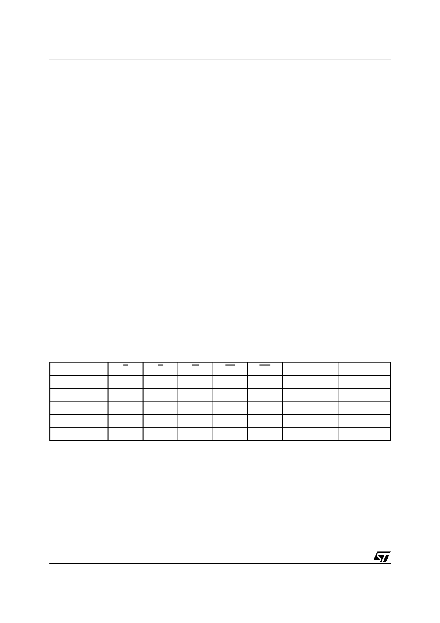
Table 2. Bus Operations
Note: X = VIL or VIH, VPPH = 12V ± 5%.
Operation
E
G
W
RP
WP
VPP
DQ0-DQ15
Bus Read
VIL
VIH
X
Don’t Care
Data Output
Bus Write
VIL
VIH
VIL
VIH
X
VDD or VPPH
Data Input
Output Disable
VIL
VIH
X
Don’t Care
Hi-Z
Standby
VIH
XX
VIH
X
Don’t Care
Hi-Z
Reset
X
VIL
X
Don’t Care
Hi-Z
相关PDF资料 |
PDF描述 |
|---|---|
| M28W640ECT85N1 | 4M X 16 FLASH 3V PROM, 85 ns, PDSO48 |
| M28W640ECT85ZB1T | 4M X 16 FLASH 3V PROM, 85 ns, PBGA48 |
| M28W640ECT70ZB1E | 4M X 16 FLASH 3V PROM, 70 ns, PBGA48 |
| M28W640ECT85N1E | 4M X 16 FLASH 3V PROM, 85 ns, PDSO48 |
| M29W040B70N1E | 4 Mbit 512Kb x8, Uniform Block Low Voltage Single Supply Flash Memory |
相关代理商/技术参数 |
参数描述 |
|---|---|
| M28W640FCB70N6 | 制造商:STMicroelectronics 功能描述: |
| M28W640FCB70N6E | 功能描述:闪存 STD FLASH 64 MEG RoHS:否 制造商:ON Semiconductor 数据总线宽度:1 bit 存储类型:Flash 存储容量:2 MB 结构:256 K x 8 定时类型: 接口类型:SPI 访问时间: 电源电压-最大:3.6 V 电源电压-最小:2.3 V 最大工作电流:15 mA 工作温度:- 40 C to + 85 C 安装风格:SMD/SMT 封装 / 箱体: 封装:Reel |
| M28W640FCB70N6F | 功能描述:闪存 STD FLASH 64 MEG RoHS:否 制造商:ON Semiconductor 数据总线宽度:1 bit 存储类型:Flash 存储容量:2 MB 结构:256 K x 8 定时类型: 接口类型:SPI 访问时间: 电源电压-最大:3.6 V 电源电压-最小:2.3 V 最大工作电流:15 mA 工作温度:- 40 C to + 85 C 安装风格:SMD/SMT 封装 / 箱体: 封装:Reel |
| M28W640FCB70ZB6E | 功能描述:闪存 STD FLASH 64 MEG RoHS:否 制造商:ON Semiconductor 数据总线宽度:1 bit 存储类型:Flash 存储容量:2 MB 结构:256 K x 8 定时类型: 接口类型:SPI 访问时间: 电源电压-最大:3.6 V 电源电压-最小:2.3 V 最大工作电流:15 mA 工作温度:- 40 C to + 85 C 安装风格:SMD/SMT 封装 / 箱体: 封装:Reel |
| M28W640FCB70ZB6F | 功能描述:闪存 STD FLASH 64 MEG RoHS:否 制造商:ON Semiconductor 数据总线宽度:1 bit 存储类型:Flash 存储容量:2 MB 结构:256 K x 8 定时类型: 接口类型:SPI 访问时间: 电源电压-最大:3.6 V 电源电压-最小:2.3 V 最大工作电流:15 mA 工作温度:- 40 C to + 85 C 安装风格:SMD/SMT 封装 / 箱体: 封装:Reel |
发布紧急采购,3分钟左右您将得到回复。