- 您现在的位置:买卖IC网 > PDF目录359020 > M295V800AB90M1T (意法半导体) Circular Connector; No. of Contacts:37; Series:JT02R; Body Material:Aluminum; Connecting Termination:Crimp; Connector Shell Size:14; Circular Contact Gender:Socket; Circular Shell Style:Box Mount Receptacle; Insert Arrangement:14-35 PDF资料下载
参数资料
| 型号: | M295V800AB90M1T |
| 厂商: | 意法半导体 |
| 元件分类: | 圆形连接器 |
| 英文描述: | Circular Connector; No. of Contacts:37; Series:JT02R; Body Material:Aluminum; Connecting Termination:Crimp; Connector Shell Size:14; Circular Contact Gender:Socket; Circular Shell Style:Box Mount Receptacle; Insert Arrangement:14-35 |
| 中文描述: | 8兆1兆x8或512KB的x16插槽,启动座单电源闪存 |
| 文件页数: | 8/21页 |
| 文件大小: | 142K |
| 代理商: | M295V800AB90M1T |
M29F800AT, M29F800AB
8/21
Chip Erase Command.
The Chip Erase com-
mand canbeused to erasethe entirechip. Six Bus
Write operations are required to issue the Chip
Erase Command and start the Program/Erase
Controller.
If any blocks are protected then these are ignored
and all the other blocks are erased. If all of the
blocks are protected the Chip Erase operation ap-
pears tostart but will terminate withinabout100
μ
s,
leaving the data unchanged. No error condition is
given when protected blocks are ignored.
During the erase operation the memory will ignore
all commands. It is not possible to issue any com-
mand to abort the operation. Typical chip erase
times are given in Table 6. All Bus Read opera-
tions during the Chip Erase operation will output
the Status Register on the Data Inputs/Outputs.
See the section on the Status Register for more
details.
After the Chip Erase operation has completed the
memory will return to the Read Mode, unless an
error has occurred. When an error occurs the
memory will continue to output the Status Regis-
ter. ARead/Reset command must be issued to re-
set the error condition and return to Read Mode.
The Chip Erase Command sets allof thebits in un-
protected blocks of the memory to ’1’. All previous
data is lost.
Block Erase Command.
The Block Erase com-
mand can be used to erase a list of one or more
blocks. Six Bus Write operations are required to
select the first block in the list. Each additional
block in the list can be selected by repeating the
sixth Bus Write operation using the address of the
additional block. The Block Erase operation starts
the Program/Erase Controller about 50
μ
s after the
last Bus Write operation. Oncethe Program/Erase
Controller starts it is not possible to select any
more blocks. Each additional block must therefore
be selected within 50
μ
s of the last block. The 50
μ
s
timer restartswhen an additionalblock is selected.
The Status Register can be read after the sixth
Bus Write operation. See the Status Register for
details on how to identify if the Program/Erase
Controller has started the Block Erase operation.
If any selected blocksare protected then these are
ignored and all the other selected blocks are
erased. If all of the selected blocks are protected
the Block Erase operation appears to start but will
terminate within about 100
μ
s, leaving the data un-
changed. No errorcondition is given when protect-
ed blocks are ignored.
During the Block Erase operation the memory will
ignore all commands except the Erase Suspend
and Read/Reset commands. Typical block erase
times are given in Table 6. All Bus Read opera-
tions during the Block Erase operation will output
the Status Register on the Data Inputs/Outputs.
See the section on the Status Register for more
details.
After the Block Erase operation has completedthe
memory will return to the Read Mode, unless an
error has occurred. When an error occurs the
memory will continue to output the Status Regis-
ter. A Read/Reset command must be issued to re-
set the error condition and return to Read mode.
The Block Erase Command sets all of the bits in
the unprotected selected blocks to ’1’. All previous
data in the selected blocks is lost.
Erase Suspend Command.
The Erase Suspend
Command may be used to temporarily suspend a
Block Erase operation and return the memory to
Read mode. The command requires one Bus
Write operation.
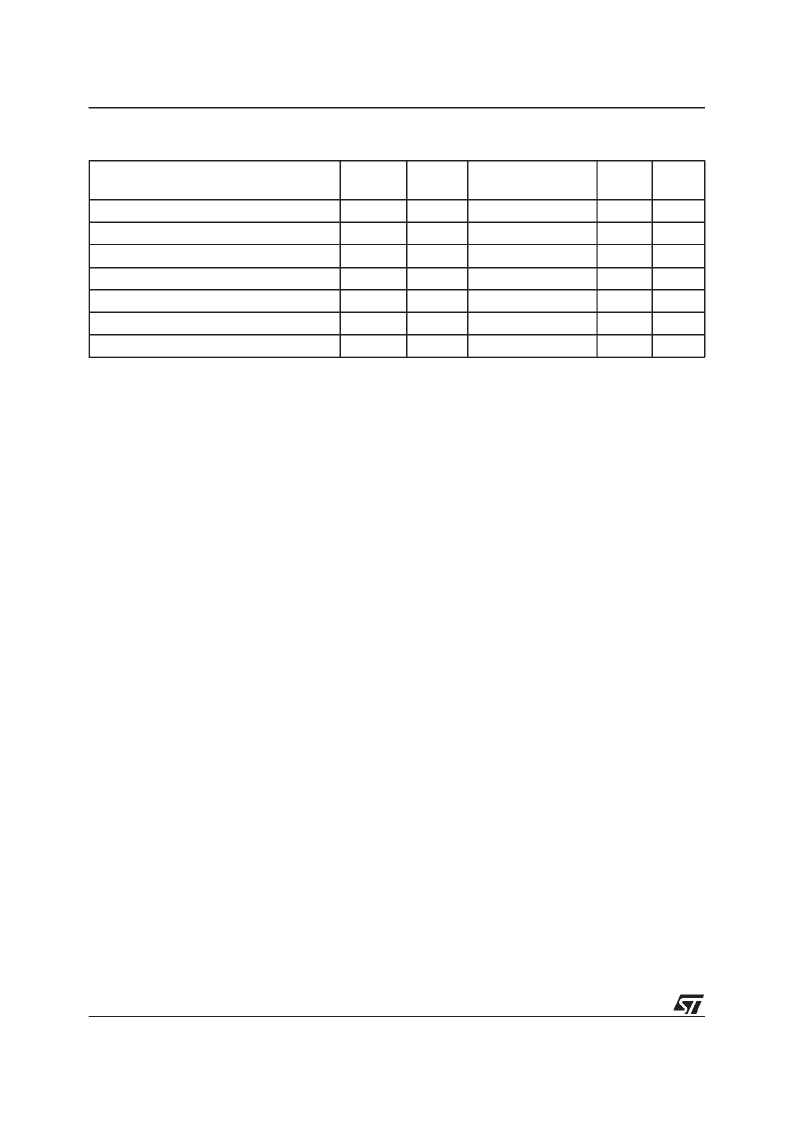
Table 6. Program, Erase Times and Program, Erase Endurance Cycles
(T
A
= 0 to 70
°
C, –40 to 85
°
C or –40 to 125
°
C)
Note: 1. T
A
= 25
°
C, V
CC
= 5V.
Parameter
Min
Typ
(1)
Typical after
100k W/E Cycles
(1)
Max
Unit
Chip Erase (All bits in the memory set to ‘0’)
3
3
sec
Chip Erase
8
8
30
sec
Block Erase (64 Kbytes)
0.6
0.6
4
sec
Program (Byte or Word)
8
8
150
μ
s
Chip Program (Byte by Byte)
9
9
35
sec
Chip Program (Word by Word)
4.5
4.5
18
sec
Program/Erase Cycles (per Block)
100,000
cycles
相关PDF资料 |
PDF描述 |
|---|---|
| M29DW128F60NF1 | 128 Mbit (16Mb x8 or 8Mb x16, Multiple Bank, Page, Boot Block) 3V Supply, Flash Memory |
| M29DW128F60NF1E | 128 Mbit (16Mb x8 or 8Mb x16, Multiple Bank, Page, Boot Block) 3V Supply, Flash Memory |
| M29DW128F60NF1F | 128 Mbit (16Mb x8 or 8Mb x16, Multiple Bank, Page, Boot Block) 3V Supply, Flash Memory |
| M29DW128F60NF1T | 128 Mbit (16Mb x8 or 8Mb x16, Multiple Bank, Page, Boot Block) 3V Supply, Flash Memory |
| M29DW128F60NF6 | 128 Mbit (16Mb x8 or 8Mb x16, Multiple Bank, Page, Boot Block) 3V Supply, Flash Memory |
相关代理商/技术参数 |
参数描述 |
|---|---|
| M295V800AB90M3T | 制造商:STMICROELECTRONICS 制造商全称:STMicroelectronics 功能描述:8 Mbit 1Mb x8 or 512Kb x16, Boot Block Single Supply Flash Memory |
| M295V800AB90M6T | 制造商:STMICROELECTRONICS 制造商全称:STMicroelectronics 功能描述:8 Mbit 1Mb x8 or 512Kb x16, Boot Block Single Supply Flash Memory |
| M295V800AB90N1T | 制造商:STMICROELECTRONICS 制造商全称:STMicroelectronics 功能描述:8 Mbit 1Mb x8 or 512Kb x16, Boot Block Single Supply Flash Memory |
| M295V800AB90N3T | 制造商:STMICROELECTRONICS 制造商全称:STMicroelectronics 功能描述:8 Mbit 1Mb x8 or 512Kb x16, Boot Block Single Supply Flash Memory |
| M295V800AB90N6T | 制造商:STMICROELECTRONICS 制造商全称:STMicroelectronics 功能描述:8 Mbit 1Mb x8 or 512Kb x16, Boot Block Single Supply Flash Memory |
发布紧急采购,3分钟左右您将得到回复。