- 您现在的位置:买卖IC网 > PDF目录69010 > M34501M2-XXXFP 4-BIT, MROM, MICROCONTROLLER, PDSO20 PDF资料下载
参数资料
| 型号: | M34501M2-XXXFP |
| 元件分类: | 微控制器/微处理器 |
| 英文描述: | 4-BIT, MROM, MICROCONTROLLER, PDSO20 |
| 封装: | 5.30 X 12.60 MM, 1.27 MM PITCH, PLASTIC, SOP-20 |
| 文件页数: | 48/118页 |
| 文件大小: | 952K |
| 代理商: | M34501M2-XXXFP |
第1页第2页第3页第4页第5页第6页第7页第8页第9页第10页第11页第12页第13页第14页第15页第16页第17页第18页第19页第20页第21页第22页第23页第24页第25页第26页第27页第28页第29页第30页第31页第32页第33页第34页第35页第36页第37页第38页第39页第40页第41页第42页第43页第44页第45页第46页第47页当前第48页第49页第50页第51页第52页第53页第54页第55页第56页第57页第58页第59页第60页第61页第62页第63页第64页第65页第66页第67页第68页第69页第70页第71页第72页第73页第74页第75页第76页第77页第78页第79页第80页第81页第82页第83页第84页第85页第86页第87页第88页第89页第90页第91页第92页第93页第94页第95页第96页第97页第98页第99页第100页第101页第102页第103页第104页第105页第106页第107页第108页第109页第110页第111页第112页第113页第114页第115页第116页第117页第118页
4501 Group
Rev.3.01
2005.02.07
page 33 of 112
REJ03B0104-0301
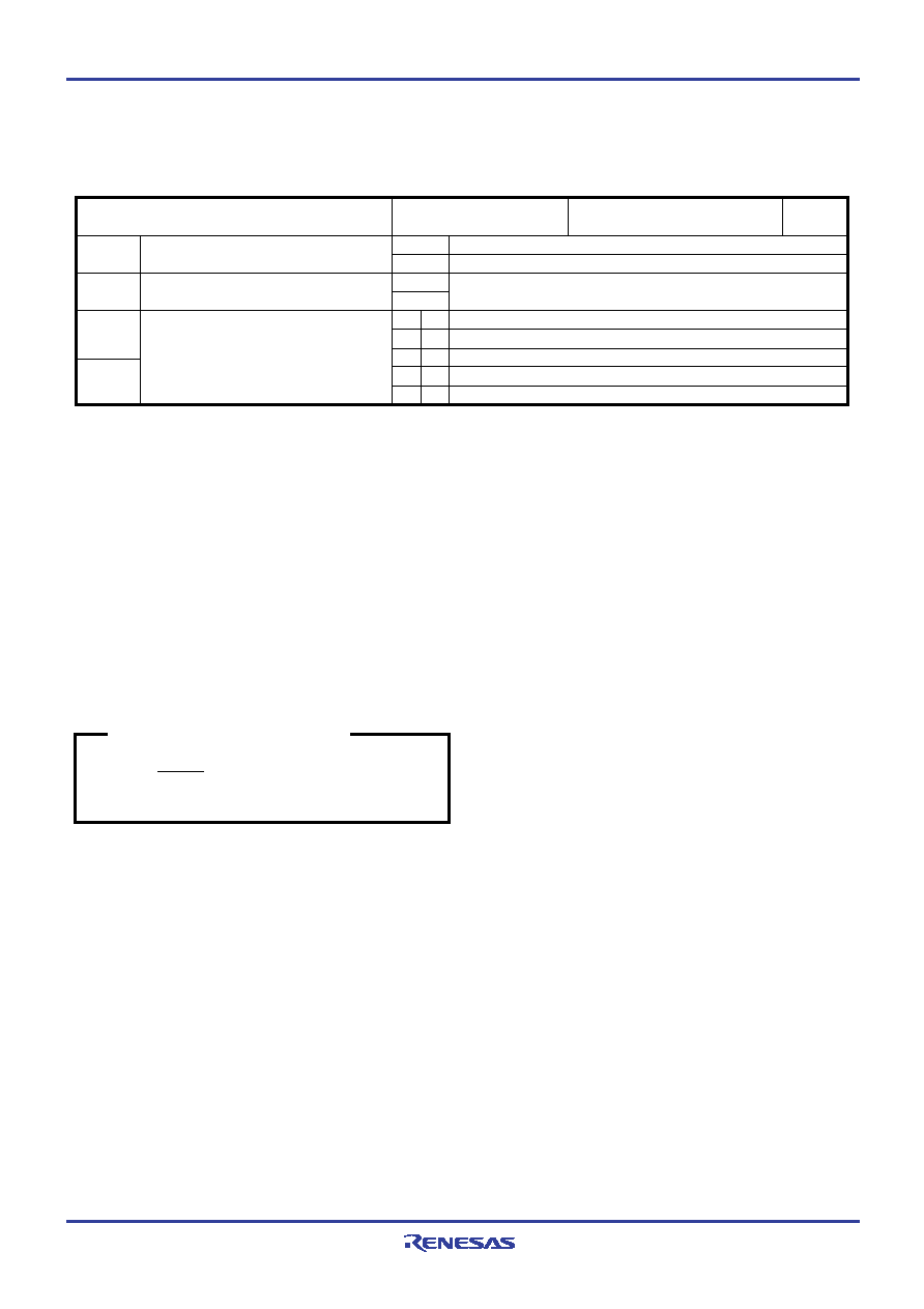
Q13
Q12
A/D control register Q1
A/D operation mode selection bit
Not used
Analog input pin selection bits
at reset : 00002
at RAM back-up : state retained
0
1
0
1
Q11
0
1
A/D conversion mode
Comparator mode
This bit has no function, but read/write is enabled.
Selected pins
AIN0
AIN1
Not available
Note: “R” represents read enabled, and “W” represents write enabled.
Q10
0
1
0
1
(1) Operating at A/D conversion mode
The A/D conversion mode is set by setting the bit 3 of register Q1 to “0.”
(2) Successive comparison register AD
Register AD stores the A/D conversion result of an analog input in
10-bit digital data format. The contents of the high-order 8 bits of
this register can be stored in register B and register A with the
TABAD instruction. The contents of the low-order 2 bits of this reg-
ister can be stored into the high-order 2 bits of register A with the
TALA instruction. However, do not execute these instructions dur-
ing A/D conversion.
When the contents of register AD is n, the logic value of the com-
parison voltage Vref generated from the built-in DA converter can
be obtained with the reference voltage VDD by the following for-
mula:
Logic value of comparison voltage Vref
Vref =
n
n: The value of register AD (n = 0 to 1023)
VDD
1024
R/W
Table 12 A/D control registers
(3) A/D conversion completion flag (ADF)
A/D conversion completion flag (ADF) is set to “1” when A/D con-
version completes. The state of ADF flag can be examined with the
skip instruction (SNZAD). Use the interrupt control register V2 to
select the interrupt or the skip instruction.
The ADF flag is cleared to “0” when the interrupt occurs or when
the next instruction is skipped with the skip instruction.
(4) A/D conversion start instruction (ADST)
A/D conversion starts when the ADST instruction is executed. The
conversion result is automatically stored in the register AD.
(5) A/D control register Q1
Register Q1 is used to select the operation mode and one of ana-
log input pins.
Q11
Q10
(6) Operation description
A/D conversion is started with the A/D conversion start instruction
(ADST). The internal operation during A/D conversion is as follows:
When the A/D conversion starts, the register AD is cleared to
“00016.”
Next, the topmost bit of the register AD is set to “1,” and the
comparison voltage Vref is compared with the analog input volt-
age VIN.
When the comparison result is Vref < VIN, the topmost bit of the
register AD remains set to “1.” When the comparison result is
Vref > VIN, it is cleared to “0.”
The 4501 Group repeats this operation to the lowermost bit of the
register AD to convert an analog value to a digital value. A/D con-
version stops after 62 machine cycles (46.5
s when f(XIN) = 4.0
MHz in high-speed mode) from the start, and the conversion result
is stored in the register AD. An A/D interrupt activated condition is
satisfied and the ADF flag is set to “1” as soon as A/D conversion
completes (Figure 29).
相关PDF资料 |
PDF描述 |
|---|---|
| M34501E4FP | 4-BIT, OTPROM, MICROCONTROLLER, PDSO20 |
| M34501M4-XXXFP | 4-BIT, MROM, MICROCONTROLLER, PDSO20 |
| M34501E4FP | 4-BIT, OTPROM, MICROCONTROLLER, PDSO20 |
| M34502M2-XXXFP | 4-BIT, MROM, MICROCONTROLLER, PDSO24 |
| M34502M4-XXXFP | 4-BIT, MROM, MICROCONTROLLER, PDSO24 |
相关代理商/技术参数 |
参数描述 |
|---|---|
| M34501M4 | 制造商:MITSUBISHI 制造商全称:Mitsubishi Electric Semiconductor 功能描述:SINGLE-CHIP 4-BIT CMOS MICROCOMPUTER |
| M34501M4-XXXFP | 制造商:MITSUBISHI 制造商全称:Mitsubishi Electric Semiconductor 功能描述:SINGLE-CHIP 4-BIT CMOS MICROCOMPUTER |
| M34502E4 | 制造商:RENESAS 制造商全称:Renesas Technology Corp 功能描述:SINGLE-CHIP 4-BIT CMOS MICROCOMPUTER |
| M34502E4FP | 制造商:RENESAS 制造商全称:Renesas Technology Corp 功能描述:4-BIT CISC SINGLE-CHIP MICROCOMPUTER 4500 SERIES |
| M34502M2 | 制造商:RENESAS 制造商全称:Renesas Technology Corp 功能描述:SINGLE-CHIP 4-BIT CMOS MICROCOMPUTER |
发布紧急采购,3分钟左右您将得到回复。