- 您现在的位置:买卖IC网 > PDF目录69010 > M34501M2-XXXFP 4-BIT, MROM, MICROCONTROLLER, PDSO20 PDF资料下载
参数资料
| 型号: | M34501M2-XXXFP |
| 元件分类: | 微控制器/微处理器 |
| 英文描述: | 4-BIT, MROM, MICROCONTROLLER, PDSO20 |
| 封装: | 5.30 X 12.60 MM, 1.27 MM PITCH, PLASTIC, SOP-20 |
| 文件页数: | 70/118页 |
| 文件大小: | 952K |
| 代理商: | M34501M2-XXXFP |
第1页第2页第3页第4页第5页第6页第7页第8页第9页第10页第11页第12页第13页第14页第15页第16页第17页第18页第19页第20页第21页第22页第23页第24页第25页第26页第27页第28页第29页第30页第31页第32页第33页第34页第35页第36页第37页第38页第39页第40页第41页第42页第43页第44页第45页第46页第47页第48页第49页第50页第51页第52页第53页第54页第55页第56页第57页第58页第59页第60页第61页第62页第63页第64页第65页第66页第67页第68页第69页当前第70页第71页第72页第73页第74页第75页第76页第77页第78页第79页第80页第81页第82页第83页第84页第85页第86页第87页第88页第89页第90页第91页第92页第93页第94页第95页第96页第97页第98页第99页第100页第101页第102页第103页第104页第105页第106页第107页第108页第109页第110页第111页第112页第113页第114页第115页第116页第117页第118页
4501 Group
Rev.3.01
2005.02.07
page 53 of 112
REJ03B0104-0301
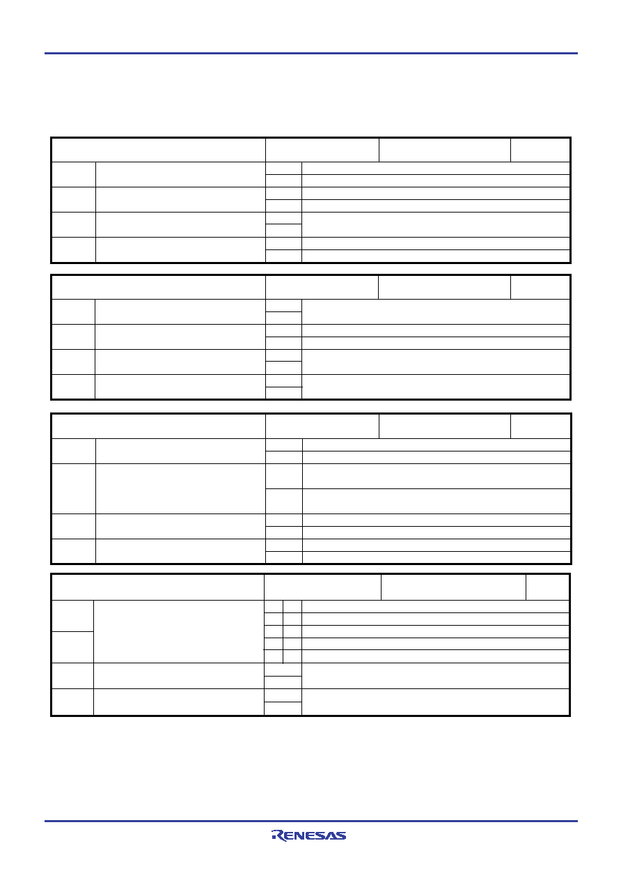
CONTROL REGISTERS
I13
I12
I11
I10
INT pin input control bit (Note 3)
Interrupt valid waveform for INT pin/
return level selection bit (Note 3)
INT pin edge detection circuit control bit
INT pin
timer 1 control enable bit
Interrupt control register I1
R/W
at RAM back-up : state retained
at reset : 00002
INT pin input disabled
INT pin input enabled
Falling waveform (“L” level of INT pin is recognized with the SNZI0
instruction)/“L” level
Rising waveform (“H” level of INT pin is recognized with the SNZI0
instruction)/“H” level
One-sided edge detected
Both edges detected
Disabled
Enabled
0
1
0
1
0
1
0
1
MR3
Clock control register MR
System clock
f(XIN) (high-speed mode)
f(XIN)/2 (middle-speed mode)
f(XIN)/4 (low-speed mode)
f(XIN)/8 (default mode)
This bit has no function, but read/write is enabled.
at reset : 11002
at RAM back-up : 11002
MR3
0
1
R/W
Not used
System clock selection bits
0
1
0
1
MR2
0
1
0
1
MR1
MR0
MR2
This bit has no function, but read/write is enabled.
Interrupt disabled (SNZAD instruction is valid)
Interrupt enabled (SNZAD instruction is invalid) (Note 2)
This bit has no function, but read/write is enabled.
R/W
V13
V12
V11
V10
V23
V22
V21
V20
Not used
A/D interrupt enable bit
Not used
Interrupt control register V2
at RAM back-up : 00002
at reset : 00002
0
1
0
1
0
1
0
1
Interrupt control register V1
Timer 2 interrupt enable bit
Timer 1 interrupt enable bit
Not used
External 0 interrupt enable bit
Interrupt disabled (SNZT2 instruction is valid)
Interrupt enabled (SNZT2 instruction is invalid) (Note 2)
Interrupt disabled (SNZT1 instruction is valid)
Interrupt enabled (SNZT1 instruction is invalid) (Note 2)
This bit has no function, but read/write is enabled.
Interrupt disabled (SNZ0 instruction is valid)
Interrupt enabled (SNZ0 instruction is invalid) (Note 2)
0
1
0
1
0
1
0
1
R/W
at RAM back-up : 00002
at reset : 00002
R/W
at RAM back-up : 00002
at reset : 00002
Notes 1: “R” represents read enabled, and “W” represents write enabled.
2: These instructions are equivalent to the NOP instruction.
3: When the contents of I12 and I13 are changed, the external interrupt request flag EXF0 may be set. Accordingly, clear EXF0 flag with the SNZ0 in-
struction when the bit 0 (V10) of register V1 to “0”. In this time, set the NOP instruction after the SNZ0 instruction, for the case when a skip is
performed with the SNZ0 instruction.
相关PDF资料 |
PDF描述 |
|---|---|
| M34501E4FP | 4-BIT, OTPROM, MICROCONTROLLER, PDSO20 |
| M34501M4-XXXFP | 4-BIT, MROM, MICROCONTROLLER, PDSO20 |
| M34501E4FP | 4-BIT, OTPROM, MICROCONTROLLER, PDSO20 |
| M34502M2-XXXFP | 4-BIT, MROM, MICROCONTROLLER, PDSO24 |
| M34502M4-XXXFP | 4-BIT, MROM, MICROCONTROLLER, PDSO24 |
相关代理商/技术参数 |
参数描述 |
|---|---|
| M34501M4 | 制造商:MITSUBISHI 制造商全称:Mitsubishi Electric Semiconductor 功能描述:SINGLE-CHIP 4-BIT CMOS MICROCOMPUTER |
| M34501M4-XXXFP | 制造商:MITSUBISHI 制造商全称:Mitsubishi Electric Semiconductor 功能描述:SINGLE-CHIP 4-BIT CMOS MICROCOMPUTER |
| M34502E4 | 制造商:RENESAS 制造商全称:Renesas Technology Corp 功能描述:SINGLE-CHIP 4-BIT CMOS MICROCOMPUTER |
| M34502E4FP | 制造商:RENESAS 制造商全称:Renesas Technology Corp 功能描述:4-BIT CISC SINGLE-CHIP MICROCOMPUTER 4500 SERIES |
| M34502M2 | 制造商:RENESAS 制造商全称:Renesas Technology Corp 功能描述:SINGLE-CHIP 4-BIT CMOS MICROCOMPUTER |
发布紧急采购,3分钟左右您将得到回复。