- 您现在的位置:买卖IC网 > PDF目录80478 > M37546G2SP 8-BIT, MROM, 8 MHz, MICROCONTROLLER, PDIP32 PDF资料下载
参数资料
| 型号: | M37546G2SP |
| 元件分类: | 微控制器/微处理器 |
| 英文描述: | 8-BIT, MROM, 8 MHz, MICROCONTROLLER, PDIP32 |
| 封装: | 8.90 X 28 MM, 1.78 MM PITCH, PLASTIC, SDIP-32 |
| 文件页数: | 14/105页 |
| 文件大小: | 1105K |
| 代理商: | M37546G2SP |
第1页第2页第3页第4页第5页第6页第7页第8页第9页第10页第11页第12页第13页当前第14页第15页第16页第17页第18页第19页第20页第21页第22页第23页第24页第25页第26页第27页第28页第29页第30页第31页第32页第33页第34页第35页第36页第37页第38页第39页第40页第41页第42页第43页第44页第45页第46页第47页第48页第49页第50页第51页第52页第53页第54页第55页第56页第57页第58页第59页第60页第61页第62页第63页第64页第65页第66页第67页第68页第69页第70页第71页第72页第73页第74页第75页第76页第77页第78页第79页第80页第81页第82页第83页第84页第85页第86页第87页第88页第89页第90页第91页第92页第93页第94页第95页第96页第97页第98页第99页第100页第101页第102页第103页第104页第105页
REJ03B0160-0122 Rev.1.22 Mar 13, 2009
page 14 of 100
7546 Group
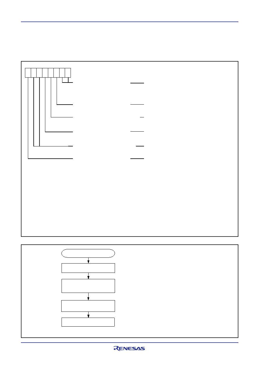
[CPU mode register] CPUM
The CPU mode register contains the stack page selection bit, etc..
This register is allocated at address 003B16.
Some function of the CPU mode register can be controlled by the
function set ROM data 2.
Fig. 12 Switching method of CPU mode register
Fig. 11 Structure of CPU mode register
Oscillation mode selection bit (Note 1, Note 4)
0 : Ceramic oscillation
1 : RC oscillation
CPU mode register (Note 1)
(CPUM: address 003B16, initial value: 8016)
Stack page selection bit
0 : 0 page
1 : 1 page
Clock division ratio selection bits
b7 b6
0
0 : f(φ) = f(XIN)/2 (High-speed mode)
0
1 : f(φ) = f(XIN)/8 (Middle-speed mode)
1
0 : applied from on-chip oscillator
1
1 : f(φ) = f(XIN)/1 (Double-speed mode)(Note 5)
On-chip oscillator oscillation control bit (Note 3)
0 : On-chip oscillator oscillation enabled
1 : On-chip oscillator oscillation stop
XIN oscillation control bit
0 : Ceramic or RC oscillation enabled
1 : Ceramic or RC oscillation stop
Processor mode bits
b1 b0
0
0 Single-chip mode
0
1 Not available
1
0 Not available
1
1 Not available
Note 1: When the setting by the function set ROM data 2 (FSROM2) is performed, the initial value of CPUM is changed
after releasing reset since bit 5 of CPUM is fixed.
2: The setting values of FSROM2 become valid by setting “0” to bit 0 of function set ROM data 0 (FSROM0).
The setting values of FSROM2 are invalid by setting “1” to this bit.
(In order that FSROM2 is invalid, write to CPUM after releasing reset.)
3: When bit 4 of FSROM2 is set to “0”, the operation of on-chip oscillator cannot be stopped.
Since the on-chip oscillator is not stopped also in the stop mode, the dissipation current in the stop mode is increased.
4: The setting value of bit 5 of CPUM can be fixed after releasing reset by setting value of bit 5 of FSROM2.
Also, when the setting of FSROM2 is invalid, this bit can be rewritten only once after releasing reset.
After rewriting it is disable to write any data to this bit.
This bit is initialized by reset, and then, rewriting it is enabled.
5: This setting can be used only at ceramic oscillation. Do not use this at RC oscillation.
b7
b0
Control by Function set ROM data 2
(FSROM2: address FFDA16) (Note 2)
This bit function can be set by setting bit 5 of FSROM2. (Note 4)
Bit 5 of FSROM2 = 0: Bit 5 of CPUM is fixed to “0”.
Bit 5 of FSROM2 = 1: Bit 5 of CPUM is “0” or “1”.
This cannot be controlled by FSROM2.
This bit function can be set by setting bit 4 of FSROM2. (Note 3)
Bit 4 of FSROM2 = 0: Bit 3 of CPUM is fixed to “0”.
Bit 4 of FSROM2 = 1: Bit 3 of CPUM is “0” or “1”.
This cannot be controlled by FSROM2.
After releasing reset
Switch the oscillation mode
selection bit (bit 5 of CPUM)
Switch the clock division ratio
selection bits (bits 6 and 7 of CPUM)
Main routine
Start with an on-chip oscillator
An initial value is set as a ceramic oscillation mode.
When it is switched to an RC oscillation, its oscillation starts.
Select 1/1, 1/2, 1/8 or on-chip oscillator.
Wait by on-chip oscillator operation
until establishment of oscillator clock
When using a ceramic oscillation, wait until establishment of
oscillation from oscillation starts.
When using an RC oscillation, wait time is not required
basically (time to execute the instruction to switch from an
on-chip oscillator meets the requirement).
Note: After system is released from reset, an on-chip oscillator turns active automatically and system operation
is started.
Switching method of CPU mode register
Switch the CPU mode register (CPUM) at the head of program af-
ter releasing Reset in the following method.
相关PDF资料 |
PDF描述 |
|---|---|
| M38047M8-XXXHP | 8-BIT, MROM, 8.4 MHz, MICROCONTROLLER, PQFP64 |
| M102E1000.0000DL | 1000 MHz, OTHER CLOCK GENERATOR, MDIP24 |
| M102P0200.0000DL | 200 MHz, OTHER CLOCK GENERATOR, MDIP24 |
| M30201F6-FP | 16-BIT, FLASH, 10 MHz, MICROCONTROLLER, PQFP56 |
| M30800SGP | 16-BIT, MROM, 20 MHz, MICROCONTROLLER, PQFP100 |
相关代理商/技术参数 |
参数描述 |
|---|---|
| M37546G2SP#U0 | 功能描述:MCU 3/5V 8K 32-SDIP QZ-ROM RoHS:是 类别:集成电路 (IC) >> 嵌入式 - 微控制器, 系列:740/38000 标准包装:250 系列:80C 核心处理器:8051 芯体尺寸:8-位 速度:16MHz 连通性:EBI/EMI,I²C,UART/USART 外围设备:POR,PWM,WDT 输入/输出数:40 程序存储器容量:- 程序存储器类型:ROMless EEPROM 大小:- RAM 容量:256 x 8 电压 - 电源 (Vcc/Vdd):4.5 V ~ 5.5 V 数据转换器:A/D 8x10b 振荡器型:内部 工作温度:-40°C ~ 85°C 封装/外壳:68-LCC(J 形引线) 包装:带卷 (TR) |
| M37546G2-XXXGP | 制造商:RENESAS 制造商全称:Renesas Technology Corp 功能描述:SINGLE-CHIP 8-BIT CMOS MICROCOMPUTER |
| M37546G2-XXXHP | 制造商:RENESAS 制造商全称:Renesas Technology Corp 功能描述:SINGLE-CHIP 8-BIT CMOS MICROCOMPUTER |
| M37546G2-XXXSP | 制造商:RENESAS 制造商全称:Renesas Technology Corp 功能描述:SINGLE-CHIP 8-BIT CMOS MICROCOMPUTER |
| M37546G4GP | 功能描述:MCU 2/5V 16K 32-LQFP RoHS:是 类别:集成电路 (IC) >> 嵌入式 - 微控制器, 系列:740/38000 标准包装:250 系列:80C 核心处理器:8051 芯体尺寸:8-位 速度:16MHz 连通性:EBI/EMI,I²C,UART/USART 外围设备:POR,PWM,WDT 输入/输出数:40 程序存储器容量:- 程序存储器类型:ROMless EEPROM 大小:- RAM 容量:256 x 8 电压 - 电源 (Vcc/Vdd):4.5 V ~ 5.5 V 数据转换器:A/D 8x10b 振荡器型:内部 工作温度:-40°C ~ 85°C 封装/外壳:68-LCC(J 形引线) 包装:带卷 (TR) |
发布紧急采购,3分钟左右您将得到回复。