- 您现在的位置:买卖IC网 > PDF目录80478 > M37546G2SP 8-BIT, MROM, 8 MHz, MICROCONTROLLER, PDIP32 PDF资料下载
参数资料
| 型号: | M37546G2SP |
| 元件分类: | 微控制器/微处理器 |
| 英文描述: | 8-BIT, MROM, 8 MHz, MICROCONTROLLER, PDIP32 |
| 封装: | 8.90 X 28 MM, 1.78 MM PITCH, PLASTIC, SDIP-32 |
| 文件页数: | 80/105页 |
| 文件大小: | 1105K |
| 代理商: | M37546G2SP |
第1页第2页第3页第4页第5页第6页第7页第8页第9页第10页第11页第12页第13页第14页第15页第16页第17页第18页第19页第20页第21页第22页第23页第24页第25页第26页第27页第28页第29页第30页第31页第32页第33页第34页第35页第36页第37页第38页第39页第40页第41页第42页第43页第44页第45页第46页第47页第48页第49页第50页第51页第52页第53页第54页第55页第56页第57页第58页第59页第60页第61页第62页第63页第64页第65页第66页第67页第68页第69页第70页第71页第72页第73页第74页第75页第76页第77页第78页第79页当前第80页第81页第82页第83页第84页第85页第86页第87页第88页第89页第90页第91页第92页第93页第94页第95页第96页第97页第98页第99页第100页第101页第102页第103页第104页第105页
REJ03B0160-0122 Rev.1.22 Mar 13, 2009
page 74 of 100
7546 Group
NOTES ON USE
Countermeasures against noise
1. Shortest wiring length
(1) Package
Select the smallest possible package to make the total wiring
length short.
<Reason>
The wiring length depends on a microcomputer package. Use of a
small package, for example QFP and not DIP, makes the total wir-
ing length short to reduce influence of noise.
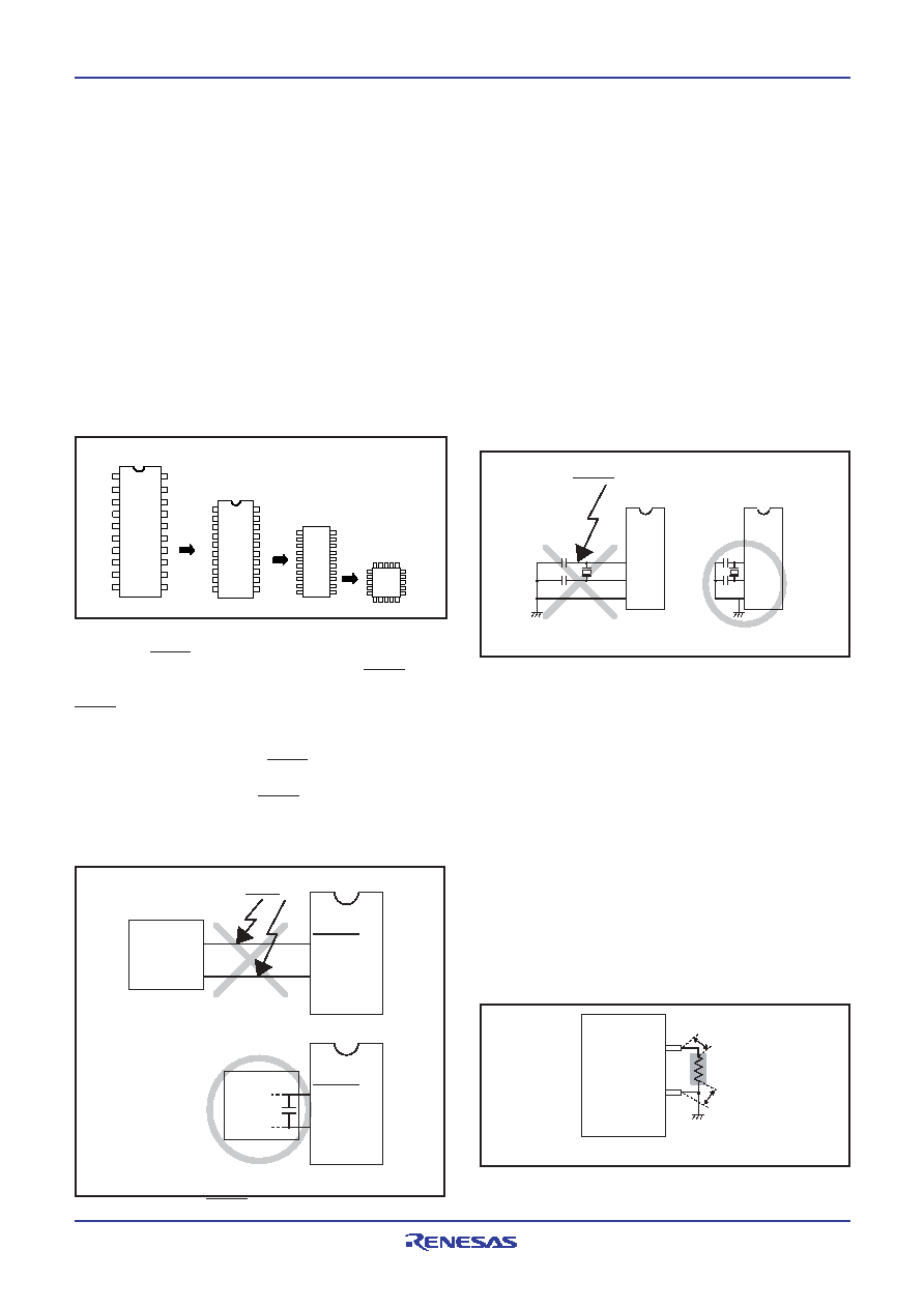
(3) Wiring for clock input/output pins
Make the length of wiring which is connected to clock I/O pins as
short as possible.
Make the length of wiring (within 20 mm) across the grounding
lead of a capacitor which is connected to an oscillator and the
VSS pin of a microcomputer as short as possible.
Separate the VSS pattern only for oscillation from other VSS pat-
terns.
<Reason>
If noise enters clock I/O pins, clock waveforms may be deformed.
This may cause a program failure or program runaway. Also, if a
potential difference is caused by the noise between the VSS level
of a microcomputer and the VSS level of an oscillator, the correct
clock will not be input in the microcomputer.
(2) Wiring for RESET pin
Make the length of wiring which is connected to the RESET pin as
short as possible. Especially, connect a capacitor across the
RESET pin and the VSS pin with the shortest possible wiring
(within 20 mm).
<Reason>
The width of a pulse input into the RESET pin is determined by the
timing necessary conditions. If noise having a shorter pulse width
than the standard is input to the RESET pin, the reset is released
before the internal state of the microcomputer is completely initial-
ized. This may cause a program runaway.
Fig. 96 Wiring for clock I/O pins
Fig. 94 Selection of packages
DIP
SDIP
SOP
QFP
Fig. 95 Wiring for the RESET pin
RESET
Reset
circuit
Noise
VSS
Reset
circuit
VSS
RESET
VSS
N.G.
O.K.
Noise
XIN
XOUT
VSS
XIN
XOUT
VSS
N.G.
O.K.
(4) Wiring to CNVSS pin
Connect CNVSS pin to a GND pattern at the shortest distance.
The GND pattern is required to be as close as possible to the
GND supplied to VSS.
In order to improve the noise reduction, to connect a 5 k resistor
serially to the CNVSS pin - GND line may be valid.
As well as the above-mentioned, in this case, connect to a GND
pattern at the shortest distance. The GND pattern is required to be
as close as possible to the GND supplied to VSS.
<Reason>
The CNVSS pin of the QzROM is the power source input pin for
the built-in QzROM. When programming in the built-in QzROM,
the impedance of the CNVSS pin is low to allow the electric cur-
rent for writing flow into the QzROM. Because of this, noise can
enter easily. If noise enters the CNVSS pin, abnormal instruction
codes or data are read from the built-in QzROM, which may cause
a program runaway.
Fig. 97 Wiring for the CNVSS pin of the QzPROM
About 5k
VSS
The shortest
CNVSS
(Note)
Note: This indicates pin.
相关PDF资料 |
PDF描述 |
|---|---|
| M38047M8-XXXHP | 8-BIT, MROM, 8.4 MHz, MICROCONTROLLER, PQFP64 |
| M102E1000.0000DL | 1000 MHz, OTHER CLOCK GENERATOR, MDIP24 |
| M102P0200.0000DL | 200 MHz, OTHER CLOCK GENERATOR, MDIP24 |
| M30201F6-FP | 16-BIT, FLASH, 10 MHz, MICROCONTROLLER, PQFP56 |
| M30800SGP | 16-BIT, MROM, 20 MHz, MICROCONTROLLER, PQFP100 |
相关代理商/技术参数 |
参数描述 |
|---|---|
| M37546G2SP#U0 | 功能描述:MCU 3/5V 8K 32-SDIP QZ-ROM RoHS:是 类别:集成电路 (IC) >> 嵌入式 - 微控制器, 系列:740/38000 标准包装:250 系列:80C 核心处理器:8051 芯体尺寸:8-位 速度:16MHz 连通性:EBI/EMI,I²C,UART/USART 外围设备:POR,PWM,WDT 输入/输出数:40 程序存储器容量:- 程序存储器类型:ROMless EEPROM 大小:- RAM 容量:256 x 8 电压 - 电源 (Vcc/Vdd):4.5 V ~ 5.5 V 数据转换器:A/D 8x10b 振荡器型:内部 工作温度:-40°C ~ 85°C 封装/外壳:68-LCC(J 形引线) 包装:带卷 (TR) |
| M37546G2-XXXGP | 制造商:RENESAS 制造商全称:Renesas Technology Corp 功能描述:SINGLE-CHIP 8-BIT CMOS MICROCOMPUTER |
| M37546G2-XXXHP | 制造商:RENESAS 制造商全称:Renesas Technology Corp 功能描述:SINGLE-CHIP 8-BIT CMOS MICROCOMPUTER |
| M37546G2-XXXSP | 制造商:RENESAS 制造商全称:Renesas Technology Corp 功能描述:SINGLE-CHIP 8-BIT CMOS MICROCOMPUTER |
| M37546G4GP | 功能描述:MCU 2/5V 16K 32-LQFP RoHS:是 类别:集成电路 (IC) >> 嵌入式 - 微控制器, 系列:740/38000 标准包装:250 系列:80C 核心处理器:8051 芯体尺寸:8-位 速度:16MHz 连通性:EBI/EMI,I²C,UART/USART 外围设备:POR,PWM,WDT 输入/输出数:40 程序存储器容量:- 程序存储器类型:ROMless EEPROM 大小:- RAM 容量:256 x 8 电压 - 电源 (Vcc/Vdd):4.5 V ~ 5.5 V 数据转换器:A/D 8x10b 振荡器型:内部 工作温度:-40°C ~ 85°C 封装/外壳:68-LCC(J 形引线) 包装:带卷 (TR) |
发布紧急采购,3分钟左右您将得到回复。