- 您现在的位置:买卖IC网 > PDF目录80446 > M38D24G6-XXXFP 8-BIT, FLASH, 6.25 MHz, MICROCONTROLLER, PQFP64 PDF资料下载
参数资料
| 型号: | M38D24G6-XXXFP |
| 元件分类: | 微控制器/微处理器 |
| 英文描述: | 8-BIT, FLASH, 6.25 MHz, MICROCONTROLLER, PQFP64 |
| 封装: | 14 X 14 MM, 0.80 MM PITCH, PLASTIC, LQFP-64 |
| 文件页数: | 17/136页 |
| 文件大小: | 2856K |
| 代理商: | M38D24G6-XXXFP |
第1页第2页第3页第4页第5页第6页第7页第8页第9页第10页第11页第12页第13页第14页第15页第16页当前第17页第18页第19页第20页第21页第22页第23页第24页第25页第26页第27页第28页第29页第30页第31页第32页第33页第34页第35页第36页第37页第38页第39页第40页第41页第42页第43页第44页第45页第46页第47页第48页第49页第50页第51页第52页第53页第54页第55页第56页第57页第58页第59页第60页第61页第62页第63页第64页第65页第66页第67页第68页第69页第70页第71页第72页第73页第74页第75页第76页第77页第78页第79页第80页第81页第82页第83页第84页第85页第86页第87页第88页第89页第90页第91页第92页第93页第94页第95页第96页第97页第98页第99页第100页第101页第102页第103页第104页第105页第106页第107页第108页第109页第110页第111页第112页第113页第114页第115页第116页第117页第118页第119页第120页第121页第122页第123页第124页第125页第126页第127页第128页第129页第130页第131页第132页第133页第134页第135页第136页
Rev.3.02
Apr 10, 2008
Page 113 of 131
REJ03B0177-0302
38D2 Group
Timing Requirements And Switching Characteristics
NOTES:
1. 80 ns in the frequency/2 mode.
2. 32 ns in the frequency/2 mode.
3. When bit 6 of address 001A16, 001F16 are “1” (clock synchronous).
Divide this value by four when bit 6 of address 001A16, 001F16 are “0” (UART).
NOTE:
1. When bit 6 of address 001A16, 001F16 are “1” (clock synchronous).
Divide this value by four when bit 6 of address 001A16, 001F16 are “0” (UART).
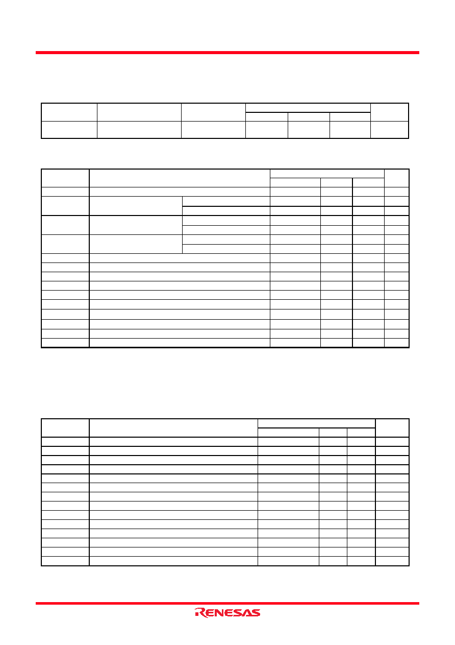
Table 43 Power supply circuit characteristics
(Vcc = 2.7 to 5.5 V, Vss = 0 V, Ta =
20 to 85°C, unless otherwise noted)
Symbol
Parameter
Test conditions
Limits
Unit
Min.
Typ.
Max.
td(P-R)
Internal power source voltage
stabilizes time at power-on
2.7
≤ VCC ≤ 5.5V
2
ms
Table 44 Timing requirements (1)
(Vcc = 4.0 to 5.5 V, Vss = 0 V, Ta =
20 to 85°C, unless otherwise noted)
Symbol
Parameter
Limits
Unit
Min.
Typ.
Max.
tW(RESET)
Reset input “L” pulse width
2
μs
tC(XIN)
Main clock input cycle time
4.5V
62.5
ns
4.0V
≤ VCC < 4.5V
125
ns
tWH(XIN)
Main clock input “H” pulse width
4.5V
25
ns
4.0V
≤ VCC < 4.5V
50
ns
tWL(XIN)
Main clock input “L” pulse width
4.5V
25
ns
4.0V
≤ VCC < 4.5V
50
ns
tC(CNTR)
CNTR0, CNTR1 input cycle time
250
ns
tWH(CNTR)
CNTR0, CNTR1 input “H” pulse width
105
ns
tWL(CNTR)
CNTR0, CNTR1 input “L” pulse width
105
ns
tWH(INT)
INT0
INT2 input “H” pulse width
80
ns
tWL(INT)
INT0
INT2 input “L” pulse width
80
ns
tC(SCLK)
Serial I/O1, 2 clock input cycle time (3)
800
ns
tWH(SCLK)
Serial I/O1, 2 clock input “H” pulse width (3)
370
ns
tWL(SCLK)
370
ns
tsu(RxD-SCLK)
Serial I/O1, 2 input setup time
220
ns
th(SCLK-RxD)
Serial I/O1, 2 input hold time
100
ns
Table 45 Timing requirements (2)
(VCC = 2.7 to 4.0 V, VSS = 0 V, Ta =
20 to 85°C, unless otherwise noted)
Symbol
Parameter
Limits
Unit
Min.
Typ.
Max.
tW(RESET)
Reset input “L” pulse width
2
μs
tC(XIN)
Main clock input cycle time (XIN input)
125
ns
tWH(XIN)
Main clock input “H” pulse width
50
ns
tWL(XIN)
Main clock input “L” pulse width
50
ns
tC(CNTR)
CNTR0, CNTR1 input cycle time
1000/VCC
ns
tWH(CNTR)
CNTR0, CNTR1 input “H” pulse width
tc(CNTR)/2
20
ns
tWL(CNTR)
CNTR0, CNTR1 input “L” pulse width
tc(CNTR)/2
20
ns
tWH(INT)
INT0
INT2 input “H” pulse width
230
ns
tWL(INT)
INT0
INT2 input “L” pulse width
230
ns
tC(SCLK)
Serial I/O1, 2 clock input cycle time
2000
ns
tWH(SCLK)
Serial I/O1, 2 clock input “H” pulse width
950
ns
tWL(SCLK)
Serial I/O1, 2 clock input “L” pulse width
950
ns
tsu(RXD-SCLK)
Serial I/O1, 2 input setup time
400
ns
th(SCLK-RXD)
Serial I/O1, 2 input hold time
200
ns
FLASH MEMORY VERSION
相关PDF资料 |
PDF描述 |
|---|---|
| MC68HC705MC4MS | 8-BIT, UVPROM, 3 MHz, MICROCONTROLLER, CDIP28 |
| MPC8270VRMHBX | 32-BIT, 266 MHz, RISC PROCESSOR, PBGA516 |
| MC9S12HZ64VFU | 16-BIT, FLASH, 25 MHz, MICROCONTROLLER, PQFP80 |
| MC6805P6P | 8-BIT, MROM, 1 MHz, MICROCONTROLLER, PDIP28 |
| MC6805S2P | 8-BIT, MROM, MICROCONTROLLER, PDIP28 |
相关代理商/技术参数 |
参数描述 |
|---|---|
| M38D24G6XXXHP | 制造商:RENESAS 制造商全称:Renesas Technology Corp 功能描述:SINGLE-CHIP 8-BIT CMOS MICROCOMPUTER |
| M38D24G7XXXFP | 制造商:RENESAS 制造商全称:Renesas Technology Corp 功能描述:SINGLE-CHIP 8-BIT CMOS MICROCOMPUTER |
| M38D24G7XXXHP | 制造商:RENESAS 制造商全称:Renesas Technology Corp 功能描述:SINGLE-CHIP 8-BIT CMOS MICROCOMPUTER |
| M38D24G8XXXFP | 制造商:RENESAS 制造商全称:Renesas Technology Corp 功能描述:SINGLE-CHIP 8-BIT CMOS MICROCOMPUTER |
| M38D24G8XXXHP | 制造商:RENESAS 制造商全称:Renesas Technology Corp 功能描述:SINGLE-CHIP 8-BIT CMOS MICROCOMPUTER |
发布紧急采购,3分钟左右您将得到回复。