- 您现在的位置:买卖IC网 > PDF目录80446 > M38D24G6-XXXFP 8-BIT, FLASH, 6.25 MHz, MICROCONTROLLER, PQFP64 PDF资料下载
参数资料
| 型号: | M38D24G6-XXXFP |
| 元件分类: | 微控制器/微处理器 |
| 英文描述: | 8-BIT, FLASH, 6.25 MHz, MICROCONTROLLER, PQFP64 |
| 封装: | 14 X 14 MM, 0.80 MM PITCH, PLASTIC, LQFP-64 |
| 文件页数: | 2/136页 |
| 文件大小: | 2856K |
| 代理商: | M38D24G6-XXXFP |
第1页当前第2页第3页第4页第5页第6页第7页第8页第9页第10页第11页第12页第13页第14页第15页第16页第17页第18页第19页第20页第21页第22页第23页第24页第25页第26页第27页第28页第29页第30页第31页第32页第33页第34页第35页第36页第37页第38页第39页第40页第41页第42页第43页第44页第45页第46页第47页第48页第49页第50页第51页第52页第53页第54页第55页第56页第57页第58页第59页第60页第61页第62页第63页第64页第65页第66页第67页第68页第69页第70页第71页第72页第73页第74页第75页第76页第77页第78页第79页第80页第81页第82页第83页第84页第85页第86页第87页第88页第89页第90页第91页第92页第93页第94页第95页第96页第97页第98页第99页第100页第101页第102页第103页第104页第105页第106页第107页第108页第109页第110页第111页第112页第113页第114页第115页第116页第117页第118页第119页第120页第121页第122页第123页第124页第125页第126页第127页第128页第129页第130页第131页第132页第133页第134页第135页第136页
Rev.3.02
Apr 10, 2008
Page 10 of 131
REJ03B0177-0302
38D2 Group
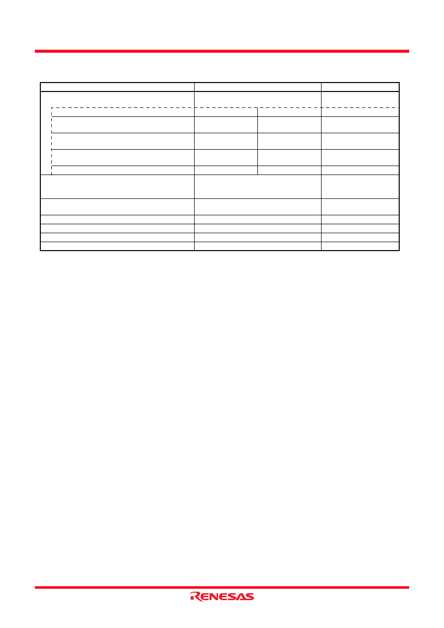
NOTE:
1. For detailed specifications, confirm the descriptions in the Datasheet.
Notes on Differences between QzROM and Flash Mem-
ory Versions
(1) The memory map, the writing modes and programming
circuits vary because of the differences in their internal
memories.
(2) The oscillation parameters of XIN-XOUT and XCIN-XCOUT
may vary.
(3) The QzROM version and the flash memory version MCUs
differ in their manufacturing processes, built-in ROM, and
layout patterns. Because of these differences, characteristic
values, operation margins, A/D conversion accuracy, noise
immunity, and noise radiation may vary within the specified
range of electrical characteristics.
(4) When switching from the flash memory version to the
QzROM version, implement system evaluations equivalent
to those implemented in the flash memory version.
(5) The both operations except the electrical characteristics are
same at the emulator (emulator MCU board: M38D29T-
RLFS).
Table 5
Differences between QzROM and flash memory versions
QzROM version
Flash memory version
Oscillation circuit at reset and at returning from stop mode
Main clock XIN or on-chip oscillator selectable
by OSCSEL pin
On-chip oscillator
Termination of OSCEL/CNVSS pin
OSCSEL = “H”
OSCSEL = “L”
CNVSS = “L”
Main clock oscillation at reset and at returning from
stop mode
Oscillation on
Stop
On-chip oscillator oscillation at reset and at returning
from stop mode
Stop
Oscillation on
System clock
φ oscillation at reset and at returning
from stop mode
f(XIN)/8
f(OCO)/32
Mounting of main clock oscillation circuit
Required
Optional
On-chip oscillator oscillation in low speed-mode
Stop
Stop by setting the on-chip
oscillator stop bit because it
is not stopped.
Writing “1” to on-chip oscillator stop bit in on-chip
oscillator mode
On-chip oscillator is stopped
On-chip oscillator is not
stopped
Reset input “L” pulse width
2
μs or more
2 ms or more
Absolute maximum rating: OSCSEL/CNVSS pin
0.3 to 8.0
0.3 to VCC + 0.3
Minimum operating power source voltage
1.8 V
2.7 V
A/D converter minimum operating power source voltage
2.0 V
2.7 V
相关PDF资料 |
PDF描述 |
|---|---|
| MC68HC705MC4MS | 8-BIT, UVPROM, 3 MHz, MICROCONTROLLER, CDIP28 |
| MPC8270VRMHBX | 32-BIT, 266 MHz, RISC PROCESSOR, PBGA516 |
| MC9S12HZ64VFU | 16-BIT, FLASH, 25 MHz, MICROCONTROLLER, PQFP80 |
| MC6805P6P | 8-BIT, MROM, 1 MHz, MICROCONTROLLER, PDIP28 |
| MC6805S2P | 8-BIT, MROM, MICROCONTROLLER, PDIP28 |
相关代理商/技术参数 |
参数描述 |
|---|---|
| M38D24G6XXXHP | 制造商:RENESAS 制造商全称:Renesas Technology Corp 功能描述:SINGLE-CHIP 8-BIT CMOS MICROCOMPUTER |
| M38D24G7XXXFP | 制造商:RENESAS 制造商全称:Renesas Technology Corp 功能描述:SINGLE-CHIP 8-BIT CMOS MICROCOMPUTER |
| M38D24G7XXXHP | 制造商:RENESAS 制造商全称:Renesas Technology Corp 功能描述:SINGLE-CHIP 8-BIT CMOS MICROCOMPUTER |
| M38D24G8XXXFP | 制造商:RENESAS 制造商全称:Renesas Technology Corp 功能描述:SINGLE-CHIP 8-BIT CMOS MICROCOMPUTER |
| M38D24G8XXXHP | 制造商:RENESAS 制造商全称:Renesas Technology Corp 功能描述:SINGLE-CHIP 8-BIT CMOS MICROCOMPUTER |
发布紧急采购,3分钟左右您将得到回复。