- 您现在的位置:买卖IC网 > PDF目录224146 > M45PE10-VMP6T (意法半导体) 4 Mbit Uniform Sector, Serial Flash Memory PDF资料下载
参数资料
| 型号: | M45PE10-VMP6T |
| 厂商: | 意法半导体 |
| 元件分类: | FLASH |
| 英文描述: | 4 Mbit Uniform Sector, Serial Flash Memory |
| 中文描述: | 4兆位统一部门,串行闪存 |
| 文件页数: | 15/34页 |
| 文件大小: | 454K |
| 代理商: | M45PE10-VMP6T |
第1页第2页第3页第4页第5页第6页第7页第8页第9页第10页第11页第12页第13页第14页当前第15页第16页第17页第18页第19页第20页第21页第22页第23页第24页第25页第26页第27页第28页第29页第30页第31页第32页第33页第34页
M45PE10
22/34
POWER-UP AND POWER-DOWN
At Power-up and Power-down, the device must
not be selected (that is Chip Select (S) must follow
the voltage applied on VCC) until VCC reaches the
correct value:
–VCC(min) at Power-up, and then for a further
delay of tVSL
–VSS at Power-down
Usually a simple pull-up resistor on Chip Select (S)
can be used to ensure safe and proper Power-up
and Power-down.
To avoid data corruption and inadvertent write op-
erations during power up, a Power On Reset
(POR) circuit is included. The logic inside the de-
vice is held reset while VCC is less than the Power
On Reset (POR) threshold value, VWI – all opera-
tions are disabled, and the device does not re-
spond to any instruction.
Moreover, the device ignores all Write Enable
(WREN), Page Write (PW), Page Program (PP),
Page Erase (PE) and Sector Erase (SE) instruc-
tions until a time delay of tPUW has elapsed after
the moment that VCC rises above the VWI thresh-
old. However, the correct operation of the device
is not guaranteed if, by this time, VCC is still below
VCC(min). No Write, Program or Erase instructions
should be sent until the later of:
–tPUW after VCC passed the VWI threshold
–tVSL after wrap roundVCC passed the
VCC(min) level
These values are specified in Table 6..
If the delay, tVSL, has elapsed, after VCC has risen
above VCC(min), the device can be selected for
READ instructions even if the tPUW delay is not yet
fully elapsed.
As an extra protection, the Reset (Reset) signal
can be driven Low for the whole duration of the
Power-up and Power-down phases.
At Power-up, the device is in the following state:
–
The device is in the Standby Power mode (not
the Deep Power-down mode).
–
The Write Enable Latch (WEL) bit is reset.
Normal precautions must be taken for supply rail
decoupling, to stabilize the VCC supply. Each de-
vice in a system should have the VCC rail decou-
pled by a suitable capacitor close to the package
pins. (Generally, this capacitor is of the order of
0.1F).
At Power-down, when VCC drops from the operat-
ing voltage, to below the Power On Reset (POR)
threshold value, VWI, all operations are disabled
and the device does not respond to any instruc-
tion. (The designer needs to be aware that if a
Power-down occurs while a Write, Program or
Erase cycle is in progress, some data corruption
can result.)
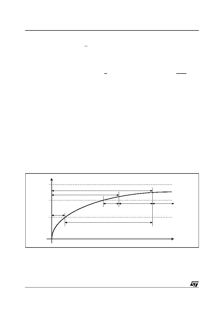
Figure 19. Power-up Timing
VCC
AI04009C
VCC(min)
VWI
Reset State
of the
Device
Chip Selection Not Allowed
Program, Erase and Write Commands are Rejected by the Device
tVSL
tPUW
time
Read Access allowed
Device fully
accessible
VCC(max)
相关PDF资料 |
PDF描述 |
|---|---|
| M45PE10-VMP6TG | 4 Mbit Uniform Sector, Serial Flash Memory |
| M45PE10-VMP6TP | 4 Mbit Uniform Sector, Serial Flash Memory |
| M464S3354BTS-C7A | 32M X 64 SYNCHRONOUS DRAM MODULE, 5.4 ns, DMA144 |
| M470T5663EH3-CF7 | DDR DRAM MODULE, ZMA200 |
| M470T6464EHS-CE6 | DDR DRAM MODULE, ZMA200 |
相关代理商/技术参数 |
参数描述 |
|---|---|
| M45PE10-VMP6TG | 功能描述:闪存 1 Mbit Lo Vltg Page Erasable Seral 闪存 RoHS:否 制造商:ON Semiconductor 数据总线宽度:1 bit 存储类型:Flash 存储容量:2 MB 结构:256 K x 8 定时类型: 接口类型:SPI 访问时间: 电源电压-最大:3.6 V 电源电压-最小:2.3 V 最大工作电流:15 mA 工作温度:- 40 C to + 85 C 安装风格:SMD/SMT 封装 / 箱体: 封装:Reel |
| M45PE10-VMP6TP | 制造商:NUMONYX 制造商全称:Numonyx B.V 功能描述:1-Mbit, page-erasable serial flash memory with byte-alterability and 75 MHz SPI bus interface |
| M45PE10-VMS6G | 制造商:Micron Technology Inc 功能描述:SERIAL NOR - Trays |
| M45PE16 | 制造商:NUMONYX 制造商全称:Numonyx B.V 功能描述:16 Mbit, low-voltage, Page-Erasable Serial Flash memory with byte alterability and a 50 MHz SPI bus interface |
| M45PE16-VMP6G | 功能描述:闪存 16 Mbit low-voltage RoHS:否 制造商:ON Semiconductor 数据总线宽度:1 bit 存储类型:Flash 存储容量:2 MB 结构:256 K x 8 定时类型: 接口类型:SPI 访问时间: 电源电压-最大:3.6 V 电源电压-最小:2.3 V 最大工作电流:15 mA 工作温度:- 40 C to + 85 C 安装风格:SMD/SMT 封装 / 箱体: 封装:Reel |
发布紧急采购,3分钟左右您将得到回复。