- 您现在的位置:买卖IC网 > PDF目录224146 > M45PE10-VMP6T (意法半导体) 4 Mbit Uniform Sector, Serial Flash Memory PDF资料下载
参数资料
| 型号: | M45PE10-VMP6T |
| 厂商: | 意法半导体 |
| 元件分类: | FLASH |
| 英文描述: | 4 Mbit Uniform Sector, Serial Flash Memory |
| 中文描述: | 4兆位统一部门,串行闪存 |
| 文件页数: | 2/34页 |
| 文件大小: | 454K |
| 代理商: | M45PE10-VMP6T |
第1页当前第2页第3页第4页第5页第6页第7页第8页第9页第10页第11页第12页第13页第14页第15页第16页第17页第18页第19页第20页第21页第22页第23页第24页第25页第26页第27页第28页第29页第30页第31页第32页第33页第34页
M45PE10
10/34
INSTRUCTIONS
All instructions, addresses and data are shifted in
and out of the device, most significant bit first.
Serial Data Input (D) is sampled on the first rising
edge of Serial Clock (C) after Chip Select (S) is
driven Low. Then, the one-byte instruction code
must be shifted in to the device, most significant bit
first, on Serial Data Input (D), each bit being
latched on the rising edges of Serial Clock (C).
The instruction set is listed in Table 4.
Every instruction sequence starts with a one-byte
instruction code. Depending on the instruction,
this might be followed by address bytes, or by data
bytes, or by both or none.
In the case of a Read Data Bytes (READ), Read
Data Bytes at Higher Speed (Fast_Read) or Read
Status Register (RDSR) instruction, the shifted-in
instruction sequence is followed by a data-out se-
quence. Chip Select (S) can be driven High after
any bit of the data-out sequence is being shifted
out.
In the case of a Page Write (PW), Page Program
(PP), Page Erase (PE), Sector Erase (SE), Write
Enable (WREN), Write Disable (WRDI), Deep
Power-down (DP) or Release from Deep Power-
down (RDP) instruction, Chip Select (S) must be
driven High exactly at a byte boundary, otherwise
the instruction is rejected, and is not executed.
That is, Chip Select (S) must driven High when the
number of clock pulses after Chip Select (S) being
driven Low is an exact multiple of eight.
All attempts to access the memory array during a
Write cycle, Program cycle or Erase cycle are ig-
nored, and the internal Write cycle, Program cycle
or Erase cycle continues unaffected.
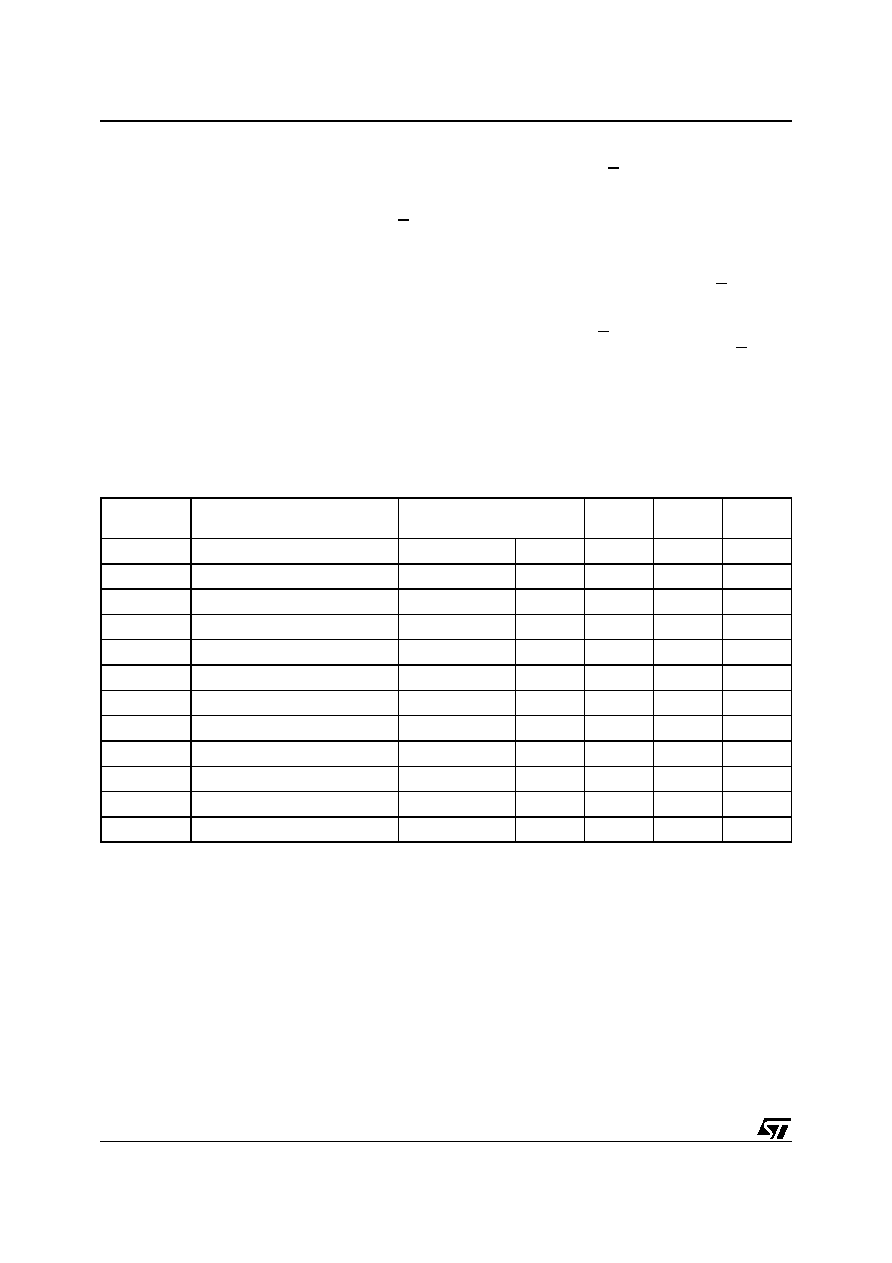
Table 4. Instruction Set
Instruction
Description
One-byte Instruction Code
Address
Bytes
Dummy
Bytes
Data
Bytes
WREN
Write Enable
0000 0110
06h
0
WRDI
Write Disable
0000 0100
04h
0
RDID
Read Identification
1001 1111
9Fh
0
1 to 3
RDSR
Read Status Register
0000 0101
05h
0
1 to
∞
READ
Read Data Bytes
0000 0011
03h
3
0
1 to
∞
FAST_READ
Read Data Bytes at Higher Speed
0000 1011
0Bh
3
1
1 to
∞
PW
Page Write
0000 1010
0Ah
3
0
1 to 256
PP
Page Program
0000 0010
02h
3
0
1 to 256
PE
Page Erase
1101 1011
DBh
3
0
SE
Sector Erase
1101 1000
D8h
3
0
DP
Deep Power-down
1011 1001
B9h
0
RDP
Release from Deep Power-down
1010 1011
ABh
0
相关PDF资料 |
PDF描述 |
|---|---|
| M45PE10-VMP6TG | 4 Mbit Uniform Sector, Serial Flash Memory |
| M45PE10-VMP6TP | 4 Mbit Uniform Sector, Serial Flash Memory |
| M464S3354BTS-C7A | 32M X 64 SYNCHRONOUS DRAM MODULE, 5.4 ns, DMA144 |
| M470T5663EH3-CF7 | DDR DRAM MODULE, ZMA200 |
| M470T6464EHS-CE6 | DDR DRAM MODULE, ZMA200 |
相关代理商/技术参数 |
参数描述 |
|---|---|
| M45PE10-VMP6TG | 功能描述:闪存 1 Mbit Lo Vltg Page Erasable Seral 闪存 RoHS:否 制造商:ON Semiconductor 数据总线宽度:1 bit 存储类型:Flash 存储容量:2 MB 结构:256 K x 8 定时类型: 接口类型:SPI 访问时间: 电源电压-最大:3.6 V 电源电压-最小:2.3 V 最大工作电流:15 mA 工作温度:- 40 C to + 85 C 安装风格:SMD/SMT 封装 / 箱体: 封装:Reel |
| M45PE10-VMP6TP | 制造商:NUMONYX 制造商全称:Numonyx B.V 功能描述:1-Mbit, page-erasable serial flash memory with byte-alterability and 75 MHz SPI bus interface |
| M45PE10-VMS6G | 制造商:Micron Technology Inc 功能描述:SERIAL NOR - Trays |
| M45PE16 | 制造商:NUMONYX 制造商全称:Numonyx B.V 功能描述:16 Mbit, low-voltage, Page-Erasable Serial Flash memory with byte alterability and a 50 MHz SPI bus interface |
| M45PE16-VMP6G | 功能描述:闪存 16 Mbit low-voltage RoHS:否 制造商:ON Semiconductor 数据总线宽度:1 bit 存储类型:Flash 存储容量:2 MB 结构:256 K x 8 定时类型: 接口类型:SPI 访问时间: 电源电压-最大:3.6 V 电源电压-最小:2.3 V 最大工作电流:15 mA 工作温度:- 40 C to + 85 C 安装风格:SMD/SMT 封装 / 箱体: 封装:Reel |
发布紧急采购,3分钟左右您将得到回复。