- 您现在的位置:买卖IC网 > PDF目录21684 > MAX17410GTM+T (Maxim Integrated)IC CTLR QPWM 2PH FOR IMV 48TQFN PDF资料下载
参数资料
| 型号: | MAX17410GTM+T |
| 厂商: | Maxim Integrated |
| 文件页数: | 38/45页 |
| 文件大小: | 0K |
| 描述: | IC CTLR QPWM 2PH FOR IMV 48TQFN |
| 产品培训模块: | Lead (SnPb) Finish for COTS Obsolescence Mitigation Program |
| 标准包装: | 2,500 |
| 系列: | * |
第1页第2页第3页第4页第5页第6页第7页第8页第9页第10页第11页第12页第13页第14页第15页第16页第17页第18页第19页第20页第21页第22页第23页第24页第25页第26页第27页第28页第29页第30页第31页第32页第33页第34页第35页第36页第37页当前第38页第39页第40页第41页第42页第43页第44页第45页
�� �
�
�Dual-Phase,� Quick-PWM� Controller�
�for� IMVP6+� CPU� Core� Power� Supplies�
�V� GS� (� TH� )� >� V� IN� ?� RSS� ?�
�Output Undervoltage Protection�
�The� output� UVP� function� is� similar� to� foldback� current�
�limiting,� but� employs� a� timer� rather� than� a� variable� cur-�
�rent� limit.� If� the� MAX17410� output� voltage� is� 400mV�
�below� the� target� voltage,� the� controller� activates� the�
�shutdown� sequence� and� sets� the� fault� latch.� Once� the�
�controller� ramps� down� to� zero,� it� forces� DL1� and� DL2�
�high,� and� pulls� DH1� and� DH2� low.� Toggle� SHDN� or�
�cycle� the� V� CC� power� supply� below� 0.5V� to� clear� the�
�fault� latch� and� reactivate� the� controller.�
�UVP� can� be� disabled� through� the� no-fault� test� mode�
�(see� the� No-Fault� Test� Mode� section).�
�Thermal-Fault� Protection�
�The� MAX17410� features� a� thermal� fault-protection� circuit.�
�When� the� junction� temperature� rises� above� +160� °� C,� a�
�thermal� sensor� sets� the� fault� latch� and� activates� the� soft-�
�shutdown� sequence.� Once� the� controller� ramps� down� to�
�zero,� it� forces� DL1� and� DL2� high,� and� pulls� DH1� and�
�DH2� low.� Toggle� SHDN� or� cycle� the� V� CC� power� supply�
�below� 0.5V� to� clear� the� fault� latch� and� reactivate� the� con-�
�troller� after� the� junction� temperature� cools� by� 15� °� C.�
�Thermal� shutdown� can� be� disabled� through� the� no-fault�
�test� mode� (see� the� No-Fault� Test� Mode� section).�
�No-Fault� Test� Mode�
�The� latched� fault-protection� features� can� complicate�
�the� process� of� debugging� prototype� breadboards� since�
�there� are� (at� most)� a� few� milliseconds� in� which� to� deter-�
�mine� what� went� wrong.� Therefore,� a� “no-fault� ”� test�
�There� must� be� a� low-resistance,� low-inductance� path�
�from� the� DL� and� DH� drivers� to� the� MOSFET� gates� for�
�the� adaptive� dead-time� circuits� to� work� properly;� other-�
�wise,� the� sense� circuitry� in� the� MAX17410� interprets� the�
�MOSFET� gates� as� “off”� while� charge� actually� remains.�
�Use� very� short,� wide� traces� (50� mils� to� 100� mils� wide� if�
�the� MOSFET� is� 1in� from� the� driver).�
�The� internal� pulldown� transistor� that� drives� DL� low� is�
�robust,� with� a� 0.25� Ω� (typ)� on-resistance.� This� helps� pre-�
�vent� DL� from� being� pulled� up� due� to� capacitive� coupling�
�from� the� drain� to� the� gate� of� the� low-side� MOSFETs�
�when� the� inductor� node� (LX)� quickly� switches� from�
�ground� to� V� IN� .� Applications� with� high� input� voltages� and�
�long� inductive� driver� traces� may� require� rising� LX� edges�
�do� not� pull� up� the� low-side� MOSFETs’� gate,� causing�
�shoot-through� currents.� The� capacitive� coupling�
�between� LX� and� DL� created� by� the� MOSFET’s� gate-to-�
�drain� capacitance� (C� RSS� ),� gate-to-source� capacitance�
�(C� ISS� -� C� RSS� ),� and� additional� board� parasitics� should�
�not� exceed� the� following� minimum� threshold:�
�?� C� ?�
�?� C� ISS� ?�
�Typically,� adding� a� 4700pF� between� DL� and� power�
�ground� (C� NL� in� Figure� 10),� close� to� the� low-side�
�MOSFETs,� greatly� reduces� coupling.� Do� not� exceed�
�22nF� of� total� gate� capacitance� to� prevent� excessive�
�turn-off� delays.�
�mode� is� provided� to� disable� the� fault� protection—over-�
�voltage� protection,� undervoltage� protection,� and� ther-�
�mal� shutdown.� Additionally,� the� test� mode� clears� the�
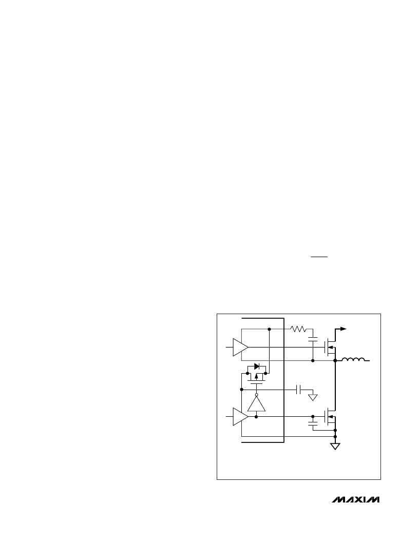
�BST_�
�(R� BST� )*�
�INPUT� (V� IN� )�
�fault� latch� if� it� has� been� set.� The� no-fault� test� mode� is�
�entered� by� forcing� 11V� to� 13V� on� SHDN� .�
�MOSFET� Gate� Drivers�
�DH_�
�LX_�
�C� BST�
�N� H�
�L�
�The� DH� and� DL� drivers� are� optimized� for� driving� moder-�
�ate-sized� high-side� and� larger� low-side� power� MOSFETs.�
�This� is� consistent� with� the� low� duty� factor� seen� in� note-�
�book� applications,� where� a� large� V� IN� -� V� OUT� differential�
�exists.� The� high-side� gate� drivers� (DH)� source� and� sink�
�2.2A,� and� the� low-side� gate� drivers� (DL)� source� 2.7A� and�
�V� DD�
�C� BYP�
�sink� 8A.� This� ensures� robust� gate� drive� for� high-current�
�applications.� The� DH_� floating� high-side� MOSFET� drivers�
�are� powered� by� internal� boost� switch� charge� pumps� at�
�BST_,� while� the� DL_� synchronous-rectifier� drivers� are�
�DL_�
�PGND�
�(C� NL� )*�
�N� L�
�powered� directly� by� the� 5V� bias� supply� (V� DD� ).�
�Adaptive� dead-time� circuits� monitor� the� DL� and� DH� dri-�
�vers� and� prevent� either� FET� from� turning� on� until� the�
�other� is� fully� off.� The� adaptive� driver� dead� time� allows�
�operation� without� shoot-through� with� a� wide� range� of�
�MOSFETs,� minimizing� delays� and� maintaining� efficiency.�
�(R� BST� )*� OPTIONAL—THE� RESISTOR� LOWERS� EMI� BY� DECREASING� THE�
�SWITCHING� NODE� RISE� TIME.�
�(C� NL� )*� OPTIONAL—THE� CAPACITOR� REDUCES� LX� TO� DL� CAPACITIVE�
�COUPLING� THAT� CAN� CAUSE� SHOOT-THROUGH� CURRENTS.�
�Figure� 10.� Gate-Drive� Circuit�
�38�
�______________________________________________________________________________________�
�相关PDF资料 |
PDF描述 |
|---|---|
| BAV99W,115 | DIODE ARRAY 100V 130MA SOT323 |
| ATS049B | CRYSTAL 4.9152 MHZ 18PF |
| ATS221B | CRYSTAL 22.1184 MHZ 18 PF FUND |
| ATS20A | CRYSTAL 20.0 MHZ 20 PF FUND |
| ATS073B | CRYSTAL 7.3728 MHZ 18 PF FUND |
相关代理商/技术参数 |
参数描述 |
|---|---|
| MAX17411GTM+ | 功能描述:电流型 PWM 控制器 IMVP7 CPU & Graphics Controller RoHS:否 制造商:Texas Instruments 开关频率:27 KHz 上升时间: 下降时间: 工作电源电压:6 V to 15 V 工作电源电流:1.5 mA 输出端数量:1 最大工作温度:+ 105 C 安装风格:SMD/SMT 封装 / 箱体:TSSOP-14 |
| MAX17411GTM+T | 功能描述:电流型 PWM 控制器 IMVP7 CPU & Graphics Controller RoHS:否 制造商:Texas Instruments 开关频率:27 KHz 上升时间: 下降时间: 工作电源电压:6 V to 15 V 工作电源电流:1.5 mA 输出端数量:1 最大工作温度:+ 105 C 安装风格:SMD/SMT 封装 / 箱体:TSSOP-14 |
| MAX17411RGTM+ | 功能描述:电流型 PWM 控制器 RoHS:否 制造商:Texas Instruments 开关频率:27 KHz 上升时间: 下降时间: 工作电源电压:6 V to 15 V 工作电源电流:1.5 mA 输出端数量:1 最大工作温度:+ 105 C 安装风格:SMD/SMT 封装 / 箱体:TSSOP-14 |
| MAX17411RGTM+T | 功能描述:电流型 PWM 控制器 RoHS:否 制造商:Texas Instruments 开关频率:27 KHz 上升时间: 下降时间: 工作电源电压:6 V to 15 V 工作电源电流:1.5 mA 输出端数量:1 最大工作温度:+ 105 C 安装风格:SMD/SMT 封装 / 箱体:TSSOP-14 |
| MAX17411RGTM+TW | 功能描述:电流型 PWM 控制器 RoHS:否 制造商:Texas Instruments 开关频率:27 KHz 上升时间: 下降时间: 工作电源电压:6 V to 15 V 工作电源电流:1.5 mA 输出端数量:1 最大工作温度:+ 105 C 安装风格:SMD/SMT 封装 / 箱体:TSSOP-14 |
发布紧急采购,3分钟左右您将得到回复。