- 您现在的位置:买卖IC网 > PDF目录10753 > MAX19711ETN+ (Maxim Integrated Products)IC ANLG FRONT END 11MSPS 56-TQFN PDF资料下载
参数资料
| 型号: | MAX19711ETN+ |
| 厂商: | Maxim Integrated Products |
| 文件页数: | 12/36页 |
| 文件大小: | 0K |
| 描述: | IC ANLG FRONT END 11MSPS 56-TQFN |
| 产品变化通告: | Product Discontinuation 09/Jun/2011 |
| 标准包装: | 43 |
| 位数: | 10 |
| 通道数: | 2 |
| 功率(瓦特): | 37.5mW |
| 电压 - 电源,模拟: | 3V |
| 电压 - 电源,数字: | 3V |
| 封装/外壳: | 56-WFQFN 裸露焊盘 |
| 供应商设备封装: | 56-TQFN-EP(7x7) |
| 包装: | 管件 |
| 产品目录页面: | 1398 (CN2011-ZH PDF) |
第1页第2页第3页第4页第5页第6页第7页第8页第9页第10页第11页当前第12页第13页第14页第15页第16页第17页第18页第19页第20页第21页第22页第23页第24页第25页第26页第27页第28页第29页第30页第31页第32页第33页第34页第35页第36页
MAX19711
10-Bit, 11Msps, Full-Duplex
Analog Front-End
2
_______________________________________________________________________________________
ABSOLUTE MAXIMUM RATINGS
Stresses beyond those listed under “Absolute Maximum Ratings” may cause permanent damage to the device. These are stress ratings only, and functional
operation of the device at these or any other conditions beyond those indicated in the operational sections of the specifications is not implied. Exposure to
absolute maximum rating conditions for extended periods may affect device reliability.
VDD to GND, OVDD to OGND ..............................-0.3V to +3.6V
GND to OGND.......................................................-0.3V to +0.3V
IAP, IAN, QAP, QAN, IDP, IDN, QDP,
QDN, DAC1, DAC2, DAC3 to GND .....................-0.3V to VDD
ADC1, ADC2 to GND.................................-0.3V to (VDD + 0.3V)
REFP, REFN, REFIN, COM to GND ...........-0.3V to (VDD + 0.3V)
AD0–AD9, DA0–DA9, SCLK, DIN, CS/WAKE,
CLK, DOUT to OGND .........................-0.3V to (OVDD + 0.3V)
Continuous Power Dissipation (TA = +70°C)
56-Pin Thin QFN-EP (derate 27.8mW/°C above +70°C) 2.22W
Thermal Resistance
θJA ..................................................36°C/W
Operating Temperature Range ...........................-40°C to +85°C
Junction Temperature ......................................................+150°C
Storage Temperature Range .............................-60°C to +150°C
Lead Temperature (soldering, 10s) .................................+300°C
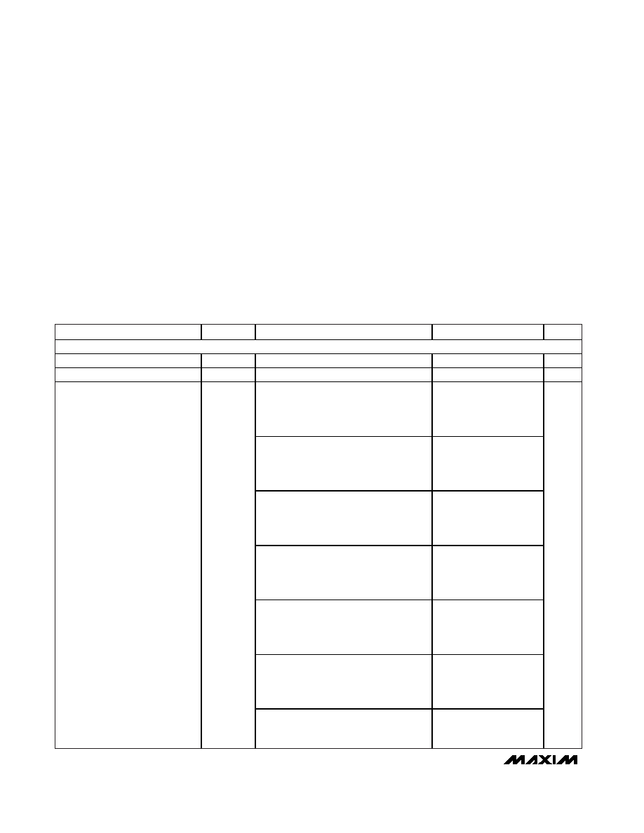
ELECTRICAL CHARACTERISTICS
(VDD = 3V, OVDD = 1.8V, internal reference (1.024V), CL
≈ 10pF on all digital outputs, fCLK = 11MHz (50% duty cycle), Rx ADC input
amplitude = -0.5dBFS, Tx DAC output amplitude = 0dBFS, VFS = 410mV, CM1 = 0, CM0 = 0, differential Rx ADC input, differential Tx
DAC output, CREFP = CREFN = CCOM = 0.33F, CL < 5pF on all aux-DAC outputs, TA = TMIN to TMAX, unless otherwise noted. Typical
values are at TA = +25°C.) (Note 1)
PARAMETER
SYMBOL
CONDITIONS
MIN
TYP
MAX
UNITS
POWER REQUIREMENTS
Analog Supply Voltage
VDD
2.7
3.0
3.3
V
Output Supply Voltage
OVDD
1.8
VDD
V
FD mode: fCLK = 11MHz, fOUT = 620kHz on
both DAC channels; fIN = 1.87MHz on both
ADC channels; aux-DACs ON and at
midscale, aux-ADC ON
14.25
17
FD mode: fCLK = 4.915MHz, fOUT =
620kHz on both DAC channels; fIN =
1.87MHz on both ADC channels; aux-
DACs ON and at midscale, aux-ADC ON
12.5
SPI2-Tx mode: fCLK = 11MHz, fOUT =
620kHz on both DAC channels; Rx ADC
OFF; aux-DACs ON and at midscale, aux-
ADC ON
11.5
14
SPI1-Rx mode: fCLK = 11MHz, fIN =
1.87MHz on both ADC channels; Tx DAC
OFF (Tx DAC outputs at 0V); aux-DACs
ON and at midscale, aux-ADC ON
8.1
10
SPI4-Tx mode: fCLK = 11MHz, fOUT =
620kHz on both DAC channels; Rx ADC
ON (output tri-stated); aux-DACs ON and
at midscale, aux-ADC ON
14.1
16.5
SPI3-Rx mode: fCLK = 11MHz, fIN =
1.87MHz on both channels; Tx DAC ON
(Tx DAC outputs at midscale); aux-DACs
ON and at midscale, aux-ADC ON
13.8
16.5
VDD Supply Current
Standby mode: CLK = 0 or OVDD;
aux-DACs ON and at midscale,
aux-ADC ON
4
mA
相关PDF资料 |
PDF描述 |
|---|---|
| V300C2M50BF3 | CONVERTER MOD DC/DC 2V 50W |
| MAX9140EXK+T | IC COMPARATOR R-R SC70-5 |
| V300C2M50BF | CONVERTER MOD DC/DC 2V 50W |
| B37950K1104K072 | CAP CER 0.1UF 100V 10% X7R 1210 |
| AD7195BCPZ | IC AFE 24BIT 4.8K 32LFSP |
相关代理商/技术参数 |
参数描述 |
|---|---|
| MAX19711ETN+ | 功能描述:ADC / DAC多通道 11Msps CODEC/AFE Full Duplex RoHS:否 制造商:Texas Instruments 转换速率: 分辨率:8 bit 接口类型:SPI 电压参考: 电源电压-最大:3.6 V 电源电压-最小:2 V 最大工作温度:+ 85 C 安装风格:SMD/SMT 封装 / 箱体:VQFN-40 |
| MAX19711ETN+T | 功能描述:ADC / DAC多通道 11Msps CODEC/AFE Full Duplex RoHS:否 制造商:Texas Instruments 转换速率: 分辨率:8 bit 接口类型:SPI 电压参考: 电源电压-最大:3.6 V 电源电压-最小:2 V 最大工作温度:+ 85 C 安装风格:SMD/SMT 封装 / 箱体:VQFN-40 |
| MAX19711ETN-T | 功能描述:ADC / DAC多通道 RoHS:否 制造商:Texas Instruments 转换速率: 分辨率:8 bit 接口类型:SPI 电压参考: 电源电压-最大:3.6 V 电源电压-最小:2 V 最大工作温度:+ 85 C 安装风格:SMD/SMT 封装 / 箱体:VQFN-40 |
| MAX19711EVCMODU+ | 功能描述:数据转换 IC 开发工具 MAX19710/13 Eval Kit RoHS:否 制造商:Texas Instruments 产品:Demonstration Kits 类型:ADC 工具用于评估:ADS130E08 接口类型:SPI 工作电源电压:- 6 V to + 6 V |
| MAX19711EVKIT | 功能描述:数据转换 IC 开发工具 RoHS:否 制造商:Texas Instruments 产品:Demonstration Kits 类型:ADC 工具用于评估:ADS130E08 接口类型:SPI 工作电源电压:- 6 V to + 6 V |
发布紧急采购,3分钟左右您将得到回复。