- 您现在的位置:买卖IC网 > PDF目录10753 > MAX19711ETN+ (Maxim Integrated Products)IC ANLG FRONT END 11MSPS 56-TQFN PDF资料下载
参数资料
| 型号: | MAX19711ETN+ |
| 厂商: | Maxim Integrated Products |
| 文件页数: | 9/36页 |
| 文件大小: | 0K |
| 描述: | IC ANLG FRONT END 11MSPS 56-TQFN |
| 产品变化通告: | Product Discontinuation 09/Jun/2011 |
| 标准包装: | 43 |
| 位数: | 10 |
| 通道数: | 2 |
| 功率(瓦特): | 37.5mW |
| 电压 - 电源,模拟: | 3V |
| 电压 - 电源,数字: | 3V |
| 封装/外壳: | 56-WFQFN 裸露焊盘 |
| 供应商设备封装: | 56-TQFN-EP(7x7) |
| 包装: | 管件 |
| 产品目录页面: | 1398 (CN2011-ZH PDF) |
第1页第2页第3页第4页第5页第6页第7页第8页当前第9页第10页第11页第12页第13页第14页第15页第16页第17页第18页第19页第20页第21页第22页第23页第24页第25页第26页第27页第28页第29页第30页第31页第32页第33页第34页第35页第36页
MAX19711
10-Bit, 11Msps, Full-Duplex
Analog Front-End
______________________________________________________________________________________
17
(IAP, QAP, IAN, and QAN) can be driven either differen-
tially or single-ended. Match the impedance of IAP and
IAN, as well as QAP and QAN, and set the input signal
common-mode voltage within the VDD / 2 (±800mV) Rx
ADC range for optimum performance.
Rx ADC System Timing Requirements
Figure 3 shows the relationship between the clock, ana-
log inputs, and the resulting output data. Channels IA
and QA are sampled on the rising edge of the clock sig-
nal (CLK) and the resulting data is multiplexed at the
AD0–AD9 outputs. Channel IA data is updated on the ris-
ing edge and channel QA data is updated on the falling
edge of CLK. Including the delay through the output
latch, the total clock-cycle latency is 5 clock cycles for
channel IA and 5.5 clock cycles for channel QA.
Digital Output Data (AD0–AD9)
AD0–AD9 are the Rx ADC digital logic outputs of the
MAX19711. The logic level is set by OVDD from 1.8V to
VDD. The digital output coding is offset binary (Table 1).
Keep the capacitive load on the digital outputs AD0–AD9
as low as possible (< 15pF) to avoid large digital currents
feeding back into the analog portion of the MAX19711
and degrading its dynamic performance. Buffers on the
digital outputs isolate the outputs from heavy capacitive
loads. Adding 100
Ω resistors in series with the digital out-
puts close to the MAX19711 will help improve ADC per-
formance. Refer to the MAX19711EVKIT schematic for an
example of the digital outputs driving a digital buffer
through 100
Ω series resistors.
During SHDN, IDLE, STBY, SPI2, and SPI4 states, digital
outputs AD0–AD9 are tri-stated.
Dual 10-Bit Tx DAC and Transmit Path
The dual 10-bit digital-to-analog converters (Tx DACs)
operate with clock speeds up to 11MHz. The Tx DAC
digital inputs, DA0–DA9, are multiplexed on a single
10-bit transmit bus. The voltage reference determines
the Tx path full-scale voltage at IDP, IDN and QDP, QDN
analog outputs. See the Reference Configurations sec-
tion for setting the reference voltage. Each Tx path out-
put channel integrates a lowpass filter tuned to meet the
CDMA spectral mask requirements.
The CDMA filters are tuned for 1.3MHz cutoff frequency
and > 64dBc image rejection at fIMAGE = 4.285MHz, fOUT
= 630kHz, and fCLK = 4.915MHz. See Figure 4 for an
illustration of the filter frequency response.
Buffer amplifiers follow the CDMA filters. The amplifier out-
puts (IDN, IDP, QDN, QDP) are biased at an adjustable
common-mode DC level and designed to drive a differen-
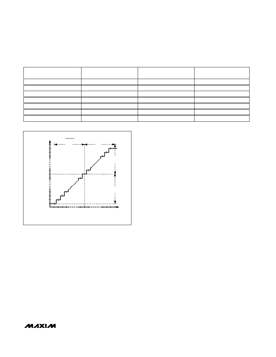
Figure 2. Rx ADC Transfer Function
INPUT VOLTAGE (LSB)
-1
-510 -509
1024
2 x VREF
1 LSB =
VREF = VREFP - VREFN
VREF
V
REF
V
REF
0+ 1
-511
+510
+512
+511
-512
+509
(COM)
OFFSET
BINAR
Y
OUTPUT
CODE
(LSB)
00 0000 0000
00 0000 0001
00 0000 0010
00 0000 0011
11 1111 1111
11 1111 1110
11 1111 1101
01 1111 1111
10 0000 0000
10 0000 0001
Table 1. Rx ADC Output Codes vs. Input Voltage
DIFFERENTIAL INPUT
VOLTAGE
DIFFERENTIAL INPUT (LSB)
OFFSET BINARY (AD0–AD9)
OUTPUT DECIMAL CODE
VREF x 512/512
511 (+Full Scale - 1 LSB)
11 1111 1111
1023
VREF x 511/512
510 (+Full Scale - 2 LSB)
11 1111 1110
1022
VREF x 1/512
+1
10 0000 0001
513
VREF x 0/512
0 (Bipolar Zero)
10 0000 0000
512
-VREF x 1/512
-1
01 1111 1111
511
-VREF x 511/512
-511 (-Full Scale +1 LSB)
00 0000 0001
1
-VREF x 512/512
-512 (-Full Scale)
00 0000 0000
0
相关PDF资料 |
PDF描述 |
|---|---|
| V300C2M50BF3 | CONVERTER MOD DC/DC 2V 50W |
| MAX9140EXK+T | IC COMPARATOR R-R SC70-5 |
| V300C2M50BF | CONVERTER MOD DC/DC 2V 50W |
| B37950K1104K072 | CAP CER 0.1UF 100V 10% X7R 1210 |
| AD7195BCPZ | IC AFE 24BIT 4.8K 32LFSP |
相关代理商/技术参数 |
参数描述 |
|---|---|
| MAX19711ETN+ | 功能描述:ADC / DAC多通道 11Msps CODEC/AFE Full Duplex RoHS:否 制造商:Texas Instruments 转换速率: 分辨率:8 bit 接口类型:SPI 电压参考: 电源电压-最大:3.6 V 电源电压-最小:2 V 最大工作温度:+ 85 C 安装风格:SMD/SMT 封装 / 箱体:VQFN-40 |
| MAX19711ETN+T | 功能描述:ADC / DAC多通道 11Msps CODEC/AFE Full Duplex RoHS:否 制造商:Texas Instruments 转换速率: 分辨率:8 bit 接口类型:SPI 电压参考: 电源电压-最大:3.6 V 电源电压-最小:2 V 最大工作温度:+ 85 C 安装风格:SMD/SMT 封装 / 箱体:VQFN-40 |
| MAX19711ETN-T | 功能描述:ADC / DAC多通道 RoHS:否 制造商:Texas Instruments 转换速率: 分辨率:8 bit 接口类型:SPI 电压参考: 电源电压-最大:3.6 V 电源电压-最小:2 V 最大工作温度:+ 85 C 安装风格:SMD/SMT 封装 / 箱体:VQFN-40 |
| MAX19711EVCMODU+ | 功能描述:数据转换 IC 开发工具 MAX19710/13 Eval Kit RoHS:否 制造商:Texas Instruments 产品:Demonstration Kits 类型:ADC 工具用于评估:ADS130E08 接口类型:SPI 工作电源电压:- 6 V to + 6 V |
| MAX19711EVKIT | 功能描述:数据转换 IC 开发工具 RoHS:否 制造商:Texas Instruments 产品:Demonstration Kits 类型:ADC 工具用于评估:ADS130E08 接口类型:SPI 工作电源电压:- 6 V to + 6 V |
发布紧急采购,3分钟左右您将得到回复。