- 您现在的位置:买卖IC网 > PDF目录10753 > MAX19711ETN+ (Maxim Integrated Products)IC ANLG FRONT END 11MSPS 56-TQFN PDF资料下载
参数资料
| 型号: | MAX19711ETN+ |
| 厂商: | Maxim Integrated Products |
| 文件页数: | 20/36页 |
| 文件大小: | 0K |
| 描述: | IC ANLG FRONT END 11MSPS 56-TQFN |
| 产品变化通告: | Product Discontinuation 09/Jun/2011 |
| 标准包装: | 43 |
| 位数: | 10 |
| 通道数: | 2 |
| 功率(瓦特): | 37.5mW |
| 电压 - 电源,模拟: | 3V |
| 电压 - 电源,数字: | 3V |
| 封装/外壳: | 56-WFQFN 裸露焊盘 |
| 供应商设备封装: | 56-TQFN-EP(7x7) |
| 包装: | 管件 |
| 产品目录页面: | 1398 (CN2011-ZH PDF) |
第1页第2页第3页第4页第5页第6页第7页第8页第9页第10页第11页第12页第13页第14页第15页第16页第17页第18页第19页当前第20页第21页第22页第23页第24页第25页第26页第27页第28页第29页第30页第31页第32页第33页第34页第35页第36页
MAX19711
10-Bit, 11Msps, Full-Duplex
Analog Front-End
______________________________________________________________________________________
27
resistive load must be greater than 200k
Ω. If capacitive
loading exceeds 5pF, then add a 10k
Ω resistor in
series with the output. Adding the series resistor helps
drive larger load capacitance (< 15pF) at the expense
of slower settling time.
10-Bit, 333ksps Auxiliary ADC
The MAX19711 integrates a 333ksps, 10-bit aux-ADC
with an input 4:1 multiplexer. In the aux-ADC mode reg-
ister, setting bit AD0 begins a conversion with the auxil-
iary ADC. Bit AD0 automatically clears when the
conversion is complete. Setting or clearing AD0 during
a conversion has no effect (see Table 13). Bit AD1
determines the internal reference of the auxiliary ADC
(see Table 14). Bits AD2 and AD3 determine the auxil-
iary ADC input source (see Table 15). Bits AD4, AD5,
and AD6 select the number of averages taken when a
single start-convert command is given. The conversion
time increases as the number of averages increases
(see Table 16). The conversion clock can be divided
down from the system clock by properly setting bits
AD7, AD8, and AD9 (see Table 17). The aux-ADC out-
put data can be written out of DOUT by setting bit
AD10 high (see Table 18).
The aux-ADC features a 4:1 input multiplexer to allow
measurements on four input sources. The input sources
are selected by AD3 and AD2 (see Table 15). Two of
the multiplexer inputs (ADC1 and ADC2) can be con-
nected to external sources such as an RF power detec-
tor like the MAX2208 or temperature sensor like the
MAX6613. The other two multiplexer inputs are internal
connections to VDD and OVDD that monitor the power-
supply voltages. The internal VDD and OVDD connec-
tions are made through integrated dividers that yield
VDD / 2 and OVDD / 2 measurement results. The aux-
ADC voltage reference can be selected between an
internal 2.048V bandgap reference or VDD (see Table
14). The VDD reference selection is provided to allow
measurement of an external voltage source with a full-
scale range extending beyond the 2.048V level. The
input source voltage range cannot extend above VDD.
The conversion requires 12 clock edges (1 for input
sampling, 1 for each of the 10 bits, and 1 at the end for
loading into the serial output register) to complete one
conversion cycle (when no averaging is being done).
Each conversion of an average (when averaging is set
greater than 1) requires 12 clock edges. The conver-
sion clock is generated from the system clock input
(CLK). An SPI-programmable divider divides the sys-
tem clock by the appropriate divisor (set with bits AD7,
AD8, and AD9; see Table 17) and provides the conver-
sion clock to the auxiliary ADC. The auxiliary ADC has a
maximum conversion rate of 333ksps. The maximum
conversion clock frequency is 4MHz (333ksps x 12
clocks). Choose the proper divider value to keep the
conversion clock frequency under 4MHz, based upon
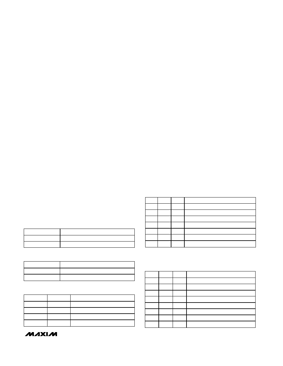
AD1
SELECTION
0
Internal 2.048V Reference (Default)
1
Internal VDD Reference
Table 14. Auxiliary ADC Reference
Table 15. Auxiliary ADC Input Source
AD3
AD2
Aux-ADC INPUT SOURCE
0
ADC1 (Default)
0
1
ADC2
10
VDD / 2
11
OVDD / 2
Table 13. Auxiliary ADC Convert
AD0
SELECTION
0
Aux-ADC Idle (Default)
1
Aux-ADC Start-Convert
Table 16. Auxiliary ADC Averaging
Table 17. Auxiliary ADC Clock (CLK)
Divider
AD6
AD5
AD4
Aux-ADC AVERAGING
00
0
1 Conversion (No Averaging) (Default)
0
1
Average of 2 Conversions
0
1
0
Average of 4 Conversions
0
1
Average of 8 Conversions
1
0
Average of 16 Conversions
1
0
1
Average of 32 Conversions
1
X
Average of 32 Conversions
AD9
AD8
AD7
Aux-ADC CONVERSION CLOCK
0
CLK Divided by 1 (Default)
0
1
CLK Divided by 2
0
1
0
CLK Divided by 4
0
1
CLK Divided by 8
1
0
CLK Divided by 16
1
0
1
CLK Divided by 32
1
0
CLK Divided by 64
1
CLK Divided by 128
X = Don’t care.
相关PDF资料 |
PDF描述 |
|---|---|
| V300C2M50BF3 | CONVERTER MOD DC/DC 2V 50W |
| MAX9140EXK+T | IC COMPARATOR R-R SC70-5 |
| V300C2M50BF | CONVERTER MOD DC/DC 2V 50W |
| B37950K1104K072 | CAP CER 0.1UF 100V 10% X7R 1210 |
| AD7195BCPZ | IC AFE 24BIT 4.8K 32LFSP |
相关代理商/技术参数 |
参数描述 |
|---|---|
| MAX19711ETN+ | 功能描述:ADC / DAC多通道 11Msps CODEC/AFE Full Duplex RoHS:否 制造商:Texas Instruments 转换速率: 分辨率:8 bit 接口类型:SPI 电压参考: 电源电压-最大:3.6 V 电源电压-最小:2 V 最大工作温度:+ 85 C 安装风格:SMD/SMT 封装 / 箱体:VQFN-40 |
| MAX19711ETN+T | 功能描述:ADC / DAC多通道 11Msps CODEC/AFE Full Duplex RoHS:否 制造商:Texas Instruments 转换速率: 分辨率:8 bit 接口类型:SPI 电压参考: 电源电压-最大:3.6 V 电源电压-最小:2 V 最大工作温度:+ 85 C 安装风格:SMD/SMT 封装 / 箱体:VQFN-40 |
| MAX19711ETN-T | 功能描述:ADC / DAC多通道 RoHS:否 制造商:Texas Instruments 转换速率: 分辨率:8 bit 接口类型:SPI 电压参考: 电源电压-最大:3.6 V 电源电压-最小:2 V 最大工作温度:+ 85 C 安装风格:SMD/SMT 封装 / 箱体:VQFN-40 |
| MAX19711EVCMODU+ | 功能描述:数据转换 IC 开发工具 MAX19710/13 Eval Kit RoHS:否 制造商:Texas Instruments 产品:Demonstration Kits 类型:ADC 工具用于评估:ADS130E08 接口类型:SPI 工作电源电压:- 6 V to + 6 V |
| MAX19711EVKIT | 功能描述:数据转换 IC 开发工具 RoHS:否 制造商:Texas Instruments 产品:Demonstration Kits 类型:ADC 工具用于评估:ADS130E08 接口类型:SPI 工作电源电压:- 6 V to + 6 V |
发布紧急采购,3分钟左右您将得到回复。