- 您现在的位置:买卖IC网 > PDF目录16753 > MAX8798ETX+ (Maxim Integrated Products)IC INTERNAL-SW BOOST REG 36-TQFN PDF资料下载
参数资料
| 型号: | MAX8798ETX+ |
| 厂商: | Maxim Integrated Products |
| 文件页数: | 2/31页 |
| 文件大小: | 0K |
| 描述: | IC INTERNAL-SW BOOST REG 36-TQFN |
| 产品培训模块: | Lead (SnPb) Finish for COTS Obsolescence Mitigation Program |
| 标准包装: | 50 |
| 应用: | LCD 监视器,笔记本电脑显示器 |
| 电流 - 电源: | 400µA |
| 电源电压: | 1.8 V ~ 6 V |
| 工作温度: | -40°C ~ 85°C |
| 安装类型: | 表面贴装 |
| 封装/外壳: | 36-WFQFN 裸露焊盘 |
| 供应商设备封装: | 36-TQFN 裸露焊盘(6x6) |
| 包装: | 管件 |
第1页当前第2页第3页第4页第5页第6页第7页第8页第9页第10页第11页第12页第13页第14页第15页第16页第17页第18页第19页第20页第21页第22页第23页第24页第25页第26页第27页第28页第29页第30页第31页
�� �
�
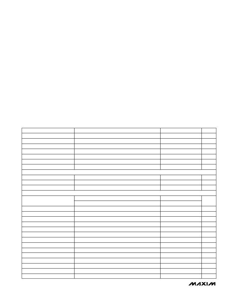
�Internal-Switch� Boost� Regulator� with�
�Integrated� 3-Channel� Scan� Driver� for� TFT� LCDs�
�ABSOLUTE� MAXIMUM� RATINGS�
�IN,� VL,� SHDN� to� AGND� .........................................-0.3V� to� +7.5V�
�V� DD� ,� SDA,� SCL,� SCLS,� WPN,� WPP,� SET� to� GND...-0.3V� to� +4.0V�
�OECON,� CPV,� OE,� STV� to� AGND..........................-0.3V� to� +4.0V�
�COMP,� FB� to� AGND� ......................................-0.3V� to� (V� L� +� 0.3V)�
�DISH� to� GND� ............................................................-6V� to� +2.0V�
�LX� to� PGND� ............................................................-0.3V� to� +20V�
�OUT,� VCOM,� NEG,� POS� to� BGND........-0.3V� to� (BOOST� +� 0.3V)�
�PGND,� BGND,� AGND� to� GND...............................-0.3V� to� +0.3V�
�GON� to� AGND� ........................................................-0.3V� to� +50V�
�GOFF� to� AGND� .............................................-30V� to� (V� IN� +� 0.3V)�
�GON� to� GOFF� ......................................................................+70V�
�CKV,� CKVB,� STVP,� CKVCS,�
�CKVBCS� to� AGND..................(GOFF� -� 0.3V)� to� (GON� +� 0.3V)�
�LX,� PGND� RMS� Current� Rating.............................................2.4A�
�Continuous� Power� Dissipation� (T� A� =� +70°C)�
�NiPd� Lead� Frame� with� Nonconductive� Epoxy�
�36-Pin,� 6mm� x� 6mm� Thin� QFN�
�(derate� 27.2mW/°C� above� +70°C)� .........................2179.8mW�
�Operating� Temperature� Range� ...........................-40°C� to� +85°C�
�Junction� Temperature� ......................................................+150°C�
�Storage� Temperature� Range� .............................-65°C� to� +150°C�
�Lead� Temperature� (soldering,� 10s)� .................................+300°C�
�BOOST� to� BGND� ....................................................-0.3V� to� +20V�
�Stresses� beyond� those� listed� under� “Absolute� Maximum� Ratings”� may� cause� permanent� damage� to� the� device.� These� are� stress� ratings� only,� and� functional�
�operation� of� the� device� at� these� or� any� other� conditions� beyond� those� indicated� in� the� operational� sections� of� the� specifications� is� not� implied.� Exposure� to�
�absolute� maximum� rating� conditions� for� extended� periods� may� affect� device� reliability.�
�ELECTRICAL� CHARACTERISTICS�
�(V� IN� =� V� DD� =� V� SHDN� =� +3V,� circuit� of� Figure� 2,� V� BOOST� =� 8V,� V� GON� =� 23V,� V� GOFF� =� -12V,� V� POS� =� 0,� V� NEG� =� 1.5V,� V� OE� =� V� CPV� =�
�V� STV� =� V� OECON� =� 0,� T� A� =� 0°C� to� +85°C� ,� unless� otherwise� noted.� Typical� values� are� at� T� A� =� +25°C.)�
�PARAMETER�
�V� DD� Input� Voltage� Range�
�CONDITIONS�
�MIN�
�1.8�
�TYP�
�MAX�
�4.0�
�UNITS�
�V�
�V� DD� Quiescent� Current�
�V� DD� Undervoltage� Lockout�
�IN� Input� Voltage� Range�
�IN� Quiescent� Current�
�IN� Undervoltage� Lockout�
�V� DD� =� 3V�
�V� DD� rising;� typical� hysteresis� 100mV�
�(Note� 1)�
�V� IN� =� 3V,� V� FB� =� 1.5V,� not� switching�
�IN� rising;� typical� hysteresis� 100mV�
�1.8�
�4�
�1.3�
�0.04�
�1.4�
�10�
�1.75�
�6.0�
�0.1�
�1.75�
�μA�
�V�
�V�
�mA�
�V�
�Rising� edge,� hysteresis� =� 15� C�
�Thermal Shutdown�
�o�
�160�
�o�
�C�
�BOOTSTRAP� LINEAR� REGULATOR� (VL)�
�VL� Output� Voltage�
�VL� Undervoltage� Lockout�
�VL� Maximum� Output� Current�
�I� VL� =� 100� μA�
�VL� rising,� typical� hysteresis� 200mV�
�V� FB� =� 1.1V�
�3.15�
�2.4�
�10�
�3.3�
�2.7�
�3.45�
�3.0�
�V�
�V�
�mA�
�MAIN� DC-DC� CONVERTER�
�BOOST� Supply� Current�
�Operating� Frequency�
�Oscillator� Maximum� Duty� Cycle�
�FB� Regulation� Voltage�
�FB� Load� Regulation�
�LX� not� switching,� no� load� on� VL�
�LX� switching,� no� load� on� VL�
�0� <� I� LOAD� <� 200mA,� transient� only�
�990�
�88�
�1.216�
�1.5�
�3�
�1170�
�92�
�1.235�
�-1�
�2�
�4�
�1350�
�96�
�1.254�
�mA�
�kHz�
�%�
�V�
�%�
�FB� Line� Regulation�
�FB� Input� Bias� Current�
�FB� Transconductance�
�FB� Voltage� Gain�
�FB� Fault� Timer� Trip� Threshold�
�LX� On-Resistance�
�LX� Leakage� Current�
�LX� Current� Limit�
�Current-Sense� Transresistance�
�V� IN� =� 1.8V� to� 5.5V,� FB� to� COMP�
�V� FB� =� 1.25V�
�I� =� 5� μA� at� COMP�
�FB� to� COMP�
�Falling� edge�
�I� LX� =� 1.2A�
�V� LX� =� 18V�
�Duty� cycle� =� 65%�
�-0.15�
�50�
�70�
�0.96�
�1.6�
�0.25�
�-0.08�
�125�
�160�
�2400�
�1�
�150�
�0.01�
�1.9�
�0.42�
�+0.15�
�200�
�280�
�1.04�
�300�
�20�
�2.2�
�0.55�
�%/V�
�nA�
�μS�
�V/V�
�V�
�m�
�μA�
�A�
�V/A�
�Soft-Start� Period�
�3�
�ms�
�2�
�_______________________________________________________________________________________�
�相关PDF资料 |
PDF描述 |
|---|---|
| 0210490404 | CABLE JUMPER 1.25MM .229M 32POS |
| A3CCB-1606M | IDC CABLE- AKC16B/AE16M/AKC16B |
| 322A134-12-0 | BOOT MOLDED |
| EBM24DCCI-S189 | CONN EDGECARD 48POS R/A .156 SLD |
| ECC22DRTN-S13 | CONN EDGECARD 44POS .100 EXTEND |
相关代理商/技术参数 |
参数描述 |
|---|---|
| MAX8798ETX+ | 功能描述:显示驱动器和控制器 Internal-Switch Boost Regulator RoHS:否 制造商:Panasonic Electronic Components 工作电源电压:2.7 V to 5.5 V 最大工作温度: 安装风格:SMD/SMT 封装 / 箱体:QFN-44 封装:Reel |
| MAX8798ETX+T | 功能描述:显示驱动器和控制器 Internal-Switch Boost Regulator RoHS:否 制造商:Panasonic Electronic Components 工作电源电压:2.7 V to 5.5 V 最大工作温度: 安装风格:SMD/SMT 封装 / 箱体:QFN-44 封装:Reel |
| MAX8798EVCMAXQU+ | 功能描述:显示开发工具 MAX8798 Eval Kit RoHS:否 制造商:4D Systems 产品:4Display Shields 工具用于评估:?OLED-160-G1, ?OLED-160-G2 接口类型:Serial 工作电源电压:5 V |
| MAX8798EVKIT+ | 功能描述:显示开发工具 MAX8798 Eval Kit RoHS:否 制造商:4D Systems 产品:4Display Shields 工具用于评估:?OLED-160-G1, ?OLED-160-G2 接口类型:Serial 工作电源电压:5 V |
| MAX8799EVKIT+ | 制造商:Maxim Integrated Products 功能描述:SINGLE-PHASE AMD CPU - Boxed Product (Development Kits) |
发布紧急采购,3分钟左右您将得到回复。