- 您现在的位置:买卖IC网 > PDF目录11658 > MC56F8002VWL (Freescale Semiconductor)DSC 12K FLASH 32MHZ 28-SOIC PDF资料下载
参数资料
| 型号: | MC56F8002VWL |
| 厂商: | Freescale Semiconductor |
| 文件页数: | 26/106页 |
| 文件大小: | 0K |
| 描述: | DSC 12K FLASH 32MHZ 28-SOIC |
| 标准包装: | 26 |
| 系列: | 56F8xxx |
| 核心处理器: | 56800E |
| 芯体尺寸: | 16-位 |
| 速度: | 32MHz |
| 连通性: | I²C,LIN,SCI,SPI |
| 外围设备: | LVD,POR,PWM,WDT |
| 输入/输出数: | 23 |
| 程序存储器容量: | 12KB(6K x 16) |
| 程序存储器类型: | 闪存 |
| RAM 容量: | 1K x 16 |
| 电压 - 电源 (Vcc/Vdd): | 1.8 V ~ 3.6 V |
| 数据转换器: | A/D 15x12b |
| 振荡器型: | 内部 |
| 工作温度: | -40°C ~ 105°C |
| 封装/外壳: | 28-SOIC(0.295",7.50mm 宽) |
| 包装: | 管件 |
| 产品目录页面: | 734 (CN2011-ZH PDF) |
| 配用: | APMOTOR56F8000E-ND - KIT DEMO MOTOR CTRL SYSTEM |
第1页第2页第3页第4页第5页第6页第7页第8页第9页第10页第11页第12页第13页第14页第15页第16页第17页第18页第19页第20页第21页第22页第23页第24页第25页当前第26页第27页第28页第29页第30页第31页第32页第33页第34页第35页第36页第37页第38页第39页第40页第41页第42页第43页第44页第45页第46页第47页第48页第49页第50页第51页第52页第53页第54页第55页第56页第57页第58页第59页第60页第61页第62页第63页第64页第65页第66页第67页第68页第69页第70页第71页第72页第73页第74页第75页第76页第77页第78页第79页第80页第81页第82页第83页第84页第85页第86页第87页第88页第89页第90页第91页第92页第93页第94页第95页第96页第97页第98页第99页第100页第101页第102页第103页第104页第105页第106页
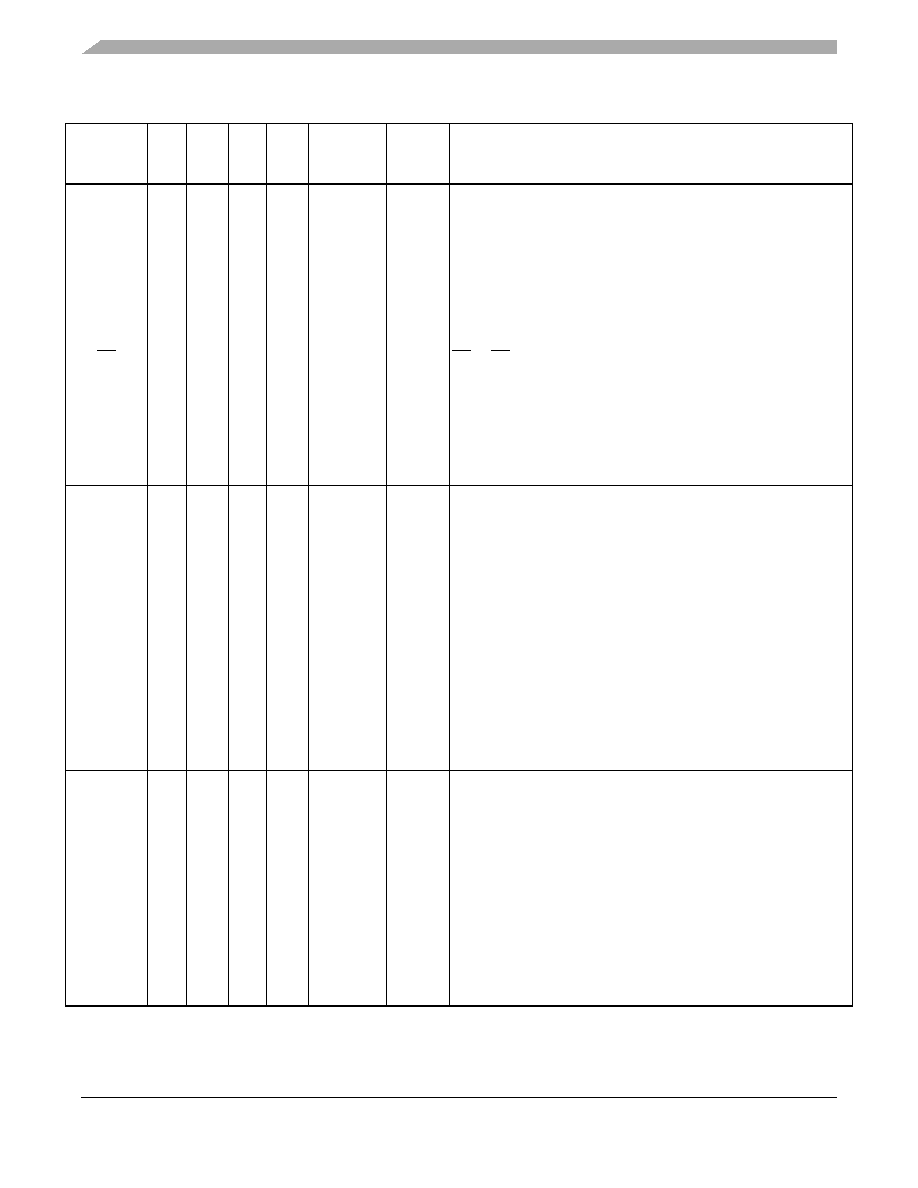
MC56F8006/MC56F8002 Digital Signal Controller, Rev. 4
Signal/Connection Descriptions
Freescale Semiconductor
26
TDI
(GPIOD0)
(ANB12)
(SS)
(TIN2)
(CMP0_
OUT)
23
30
26
45
Input
Input/
Output
Analog
Input
Output
Input,
internal
pullup
enabled
Test Data Input — This input pin provides a serial input data stream
to the JTAG/EOnCE port. It is sampled on the rising edge of TCK
and has an on-chip pullup resistor.
Port D GPIO — This GPIO pin can be individually programmed as
an input or output pin.
ANB12 — Analog input to channel 12 of ADCB
SS — SS is used in slave mode to indicate to the SPI module that
the current transfer is to be received.
TIN2 — Dual timer module channel 2 input.
CMP1_OUT — Analog comparator 1 output.
After reset, the default state is TDI.
TDO
(GPIOD1)
(ANB10)
(T0)
(CMP2_
OUT)
25
32
28
48
Output
Input/
Output
Analog
Input
Input/
Output
Output,
tri-stated,
internal
pullup
enabled
Test Data Output — This three-stateable output pin provides a serial
output data stream from the JTAG/EOnCE port. It is driven in the
shift-IR and shift-DR controller states, and changes on the falling
edge of TCK.
Port D GPIO — This GPIO pin can be individually programmed as
an input or output pin.
ANB10 — Analog input to channel 10 of ADCB.
T0 — Dual timer module channel 0 input/output.
CMP2_OUT — Analog comparator 2 output.
After reset, the default state is TDO.
TCK
(GPIOD2)
(ANA4 and
CMP1_P2)
(CMP2_
OUT)
9
14
10
22
Input
Input/
Output
Analog
Input
Output
Input,
internal
pullup
enabled
Test Clock Input — This input pin provides a gated clock to
synchronize the test logic and shift serial data to the JTAG/EOnCE
port. The pin is connected internally to a pullup resistor. A
Schmitt-trigger input is used for noise immunity.
Port D GPIO — This GPIO pin can be individually programmed as
an input or output pin.
ANA4 and CMP1_P2 — Analog input to channel 4 of ADCA and
positive input 2 of analog comparator 1.
CMP2_OUT — Analog comparator 2 output.
After reset, the default state is TCK.
Table 5. 56F8006/56F8002 Signal and Package Information (continued)
Signal
Name
28
SOIC
32
LQFP
32
PSDI
P
48
LQFP
Type
State
During
Reset
Signal Description
相关PDF资料 |
PDF描述 |
|---|---|
| VE-BNW-CU-S | CONVERTER MOD DC/DC 5.5V 200W |
| VE-BNV-CU-S | CONVERTER MOD DC/DC 5.8V 200W |
| VI-JWX-IW-F3 | CONVERTER MOD DC/DC 5.2V 100W |
| VI-JWX-IW-F2 | CONVERTER MOD DC/DC 5.2V 100W |
| MC9S08GT8AMFBE | IC MCU 8K FLASH 1K RAM 44-QFP |
相关代理商/技术参数 |
参数描述 |
|---|---|
| MC56F8002VWL | 制造商:Freescale Semiconductor 功能描述:IC DSC 16BIT 12KB 32MHZ 3.6V SOIC-28 |
| MC56F8006 | 制造商:FREESCALE 制造商全称:Freescale Semiconductor, Inc 功能描述:Digital Signal Controller |
| MC56F8006DEMO | 功能描述:开发板和工具包 - 其他处理器 MC56F8006 DEMO BOARD RoHS:否 制造商:Freescale Semiconductor 产品:Development Systems 工具用于评估:P3041 核心:e500mc 接口类型:I2C, SPI, USB 工作电源电压: |
| MC56F8006DEMO | 制造商:Freescale Semiconductor 功能描述:MC56F8006DEMO board w/o USB TAP |
| MC56F8006DEMO-T | 功能描述:开发板和工具包 - 其他处理器 MC56F8006 DEMO BOARD RoHS:否 制造商:Freescale Semiconductor 产品:Development Systems 工具用于评估:P3041 核心:e500mc 接口类型:I2C, SPI, USB 工作电源电压: |
发布紧急采购,3分钟左右您将得到回复。