- 您现在的位置:买卖IC网 > PDF目录98011 > MC56F8033VLC (FREESCALE SEMICONDUCTOR INC) 16-BIT, FLASH, 32 MHz, MICROCONTROLLER, PQFP32 PDF资料下载
参数资料
| 型号: | MC56F8033VLC |
| 厂商: | FREESCALE SEMICONDUCTOR INC |
| 元件分类: | 微控制器/微处理器 |
| 英文描述: | 16-BIT, FLASH, 32 MHz, MICROCONTROLLER, PQFP32 |
| 封装: | ROHS COMPLIANT, PLASTIC, LQFP-32 |
| 文件页数: | 56/157页 |
| 文件大小: | 2117K |
| 代理商: | MC56F8033VLC |
第1页第2页第3页第4页第5页第6页第7页第8页第9页第10页第11页第12页第13页第14页第15页第16页第17页第18页第19页第20页第21页第22页第23页第24页第25页第26页第27页第28页第29页第30页第31页第32页第33页第34页第35页第36页第37页第38页第39页第40页第41页第42页第43页第44页第45页第46页第47页第48页第49页第50页第51页第52页第53页第54页第55页当前第56页第57页第58页第59页第60页第61页第62页第63页第64页第65页第66页第67页第68页第69页第70页第71页第72页第73页第74页第75页第76页第77页第78页第79页第80页第81页第82页第83页第84页第85页第86页第87页第88页第89页第90页第91页第92页第93页第94页第95页第96页第97页第98页第99页第100页第101页第102页第103页第104页第105页第106页第107页第108页第109页第110页第111页第112页第113页第114页第115页第116页第117页第118页第119页第120页第121页第122页第123页第124页第125页第126页第127页第128页第129页第130页第131页第132页第133页第134页第135页第136页第137页第138页第139页第140页第141页第142页第143页第144页第145页第146页第147页第148页第149页第150页第151页第152页第153页第154页第155页第156页第157页
Electrical Design Considerations
56F8033/56F8023 Data Sheet, Rev. 6
Freescale Semiconductor
149
Take special care to minimize noise levels on the VREF, VDDA, and VSSA pins
Using separate power planes for VDD and VDDA and separate ground planes for VSS and VSSA are
recommended. Connect the separate analog and digital power and ground planes as close as possible to
power supply outputs. If both analog circuit and digital circuit are powered by the same power supply, it is
advisable to connect a small inductor or ferrite bead in serial with both VDDA and VSSA traces.
It is highly desirable to physically separate analog components from noisy digital components by ground
planes. Do not place an analog trace in parallel with digital traces. It is also desirable to place an analog
ground trace around an analog signal trace to isolate it from digital traces.
Because the Flash memory is programmed through the JTAG/EOnCE port, QSPI, QSCI, or I2C, the
designer should provide an interface to this port if in-circuit Flash programming is desired.
If desired, connect an external RC circuit to the RESET pin. The Resistor value should be in the range of
4.7k—10k; the Capacitor value should be in the range of 0.22f - 4.7f.
Add a 3.3k external pull-up on the TMS pin of the JTAG port to keep EOnce in a restate during normal
operation if JTAG converter is not present.
During reset and after reset but before I/O initialization, all I/O pins are at input state with internal pull-up
enable. The typical value of internal pull-up is around 110K. These internal pull-ups can be disabled by
software.
To eliminate PCB trace impedance effect, each ADC input should have a 33pf-10 ohm RC filter.
Device GPIOs have only a down (substrate) diode on the GPIO circuit. Devices do not have a positive clamp
diode because GPIOs use a floating gate structure to tolerate 5V input. The absolute maximum clamp
current is -20mA at Vin less than 0V. The continuous clamp current is -2mA at Vin less than 0V. If positive
voltage spikes are a concern, a positive clamp is recommended.
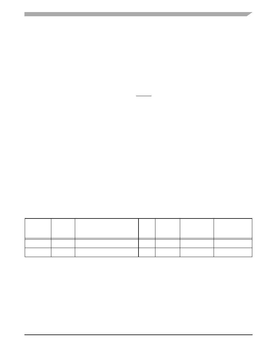
Part 13 Ordering Information
Table 13-1 lists the pertinent information needed to place an order. Consult a Freescale Semiconductor
sales office or authorized distributor to determine availability and to order devices.
* This package is RoHS compliant.
Table 13-1 56F8033/56F8023 Ordering Information
Device
Supply
Voltage
Package Type
Pin
Count
Frequency
(MHz)
Ambient
Temperature
Range
Order Number
MC56F8033
3.0–3.6 V
Low-Profile Quad Flat Pack (LQFP)
32
-40° to + 105° C
MC56F8033VLC*
MC56F8023
3.0–3.6 V
Low-Profile Quad Flat Pack (LQFP)
32
-40° to + 105° C
MC56F8023VLC*
相关PDF资料 |
PDF描述 |
|---|---|
| MC56F8347MPY60 | 16-BIT, 120 MHz, OTHER DSP, PQFP160 |
| MC56F8355VFG60 | 4-BIT, 120 MHz, OTHER DSP, PQFP128 |
| MC56F8355MFG60 | 4-BIT, 120 MHz, OTHER DSP, PQFP128 |
| MC6805R2CP | 8-BIT, MROM, MICROCONTROLLER, PDIP40 |
| MC68302PV25C | LOCAL AREA NETWORK CONTROLLER, PQFP144 |
相关代理商/技术参数 |
参数描述 |
|---|---|
| MC56F8035VLD | 功能描述:数字信号处理器和控制器 - DSP, DSC 16 BIT DSPHC 64KB RoHS:否 制造商:Microchip Technology 核心:dsPIC 数据总线宽度:16 bit 程序存储器大小:16 KB 数据 RAM 大小:2 KB 最大时钟频率:40 MHz 可编程输入/输出端数量:35 定时器数量:3 设备每秒兆指令数:50 MIPs 工作电源电压:3.3 V 最大工作温度:+ 85 C 封装 / 箱体:TQFP-44 安装风格:SMD/SMT |
| MC56F8035VLDR | 功能描述:数字信号处理器和控制器 - DSP, DSC 16 BIT DSPHC 64KB RoHS:否 制造商:Microchip Technology 核心:dsPIC 数据总线宽度:16 bit 程序存储器大小:16 KB 数据 RAM 大小:2 KB 最大时钟频率:40 MHz 可编程输入/输出端数量:35 定时器数量:3 设备每秒兆指令数:50 MIPs 工作电源电压:3.3 V 最大工作温度:+ 85 C 封装 / 箱体:TQFP-44 安装风格:SMD/SMT |
| MC56F8036 | 制造商:FREESCALE 制造商全称:Freescale Semiconductor, Inc 功能描述:16-bit Digital Signal Controllers |
| MC56F8036VLF | 功能描述:数字信号处理器和控制器 - DSP, DSC 16 BIT DSPHC RoHS:否 制造商:Microchip Technology 核心:dsPIC 数据总线宽度:16 bit 程序存储器大小:16 KB 数据 RAM 大小:2 KB 最大时钟频率:40 MHz 可编程输入/输出端数量:35 定时器数量:3 设备每秒兆指令数:50 MIPs 工作电源电压:3.3 V 最大工作温度:+ 85 C 封装 / 箱体:TQFP-44 安装风格:SMD/SMT |
| MC56F8036VLF | 制造商:Freescale Semiconductor 功能描述:IC DSC 64KB 32MHZ 3.6V LQFP-48 |
发布紧急采购,3分钟左右您将得到回复。