- 您现在的位置:买卖IC网 > PDF目录11943 > MC68HC705SR3PE (Freescale Semiconductor)IC MCU 3.75K 2.1MHZ OTP 40-DIP PDF资料下载
参数资料
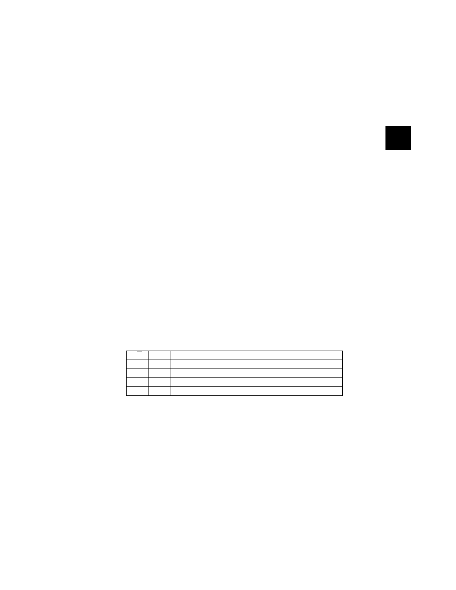
| 型号: | MC68HC705SR3PE |
| 厂商: | Freescale Semiconductor |
| 文件页数: | 20/96页 |
| 文件大小: | 0K |
| 描述: | IC MCU 3.75K 2.1MHZ OTP 40-DIP |
| 标准包装: | 9 |
| 系列: | HC05 |
| 核心处理器: | HC05 |
| 芯体尺寸: | 8-位 |
| 速度: | 4MHz |
| 外围设备: | LED,POR |
| 输入/输出数: | 32 |
| 程序存储器容量: | 3.75KB(3.75K x 8) |
| 程序存储器类型: | OTP |
| RAM 容量: | 192 x 8 |
| 电压 - 电源 (Vcc/Vdd): | 3 V ~ 5.5 V |
| 数据转换器: | A/D 4x8b |
| 振荡器型: | 内部 |
| 工作温度: | 0°C ~ 70°C |
| 封装/外壳: | 40-DIP(0.600",15.24mm) |
| 包装: | 管件 |
第1页第2页第3页第4页第5页第6页第7页第8页第9页第10页第11页第12页第13页第14页第15页第16页第17页第18页第19页当前第20页第21页第22页第23页第24页第25页第26页第27页第28页第29页第30页第31页第32页第33页第34页第35页第36页第37页第38页第39页第40页第41页第42页第43页第44页第45页第46页第47页第48页第49页第50页第51页第52页第53页第54页第55页第56页第57页第58页第59页第60页第61页第62页第63页第64页第65页第66页第67页第68页第69页第70页第71页第72页第73页第74页第75页第76页第77页第78页第79页第80页第81页第82页第83页第84页第85页第86页第87页第88页第89页第90页第91页第92页第93页第94页第95页第96页
MC68HC05SR3
Freescale
3-1
INPUT/OUTPUT PORTS
3
INPUT/OUTPUT PORTS
The MC68HC05SR3 has 32 bidirectional I/O lines, arranged as four 8-bit I/O ports (Port A, B, C,
and D). The individual bits in these ports are programmable as either inputs or outputs under
software control by the Data Direction Registers (DDRs). All port pins each has an associated
20K
pull-up resistor, which can be connected/disconnected under software control. Also, each
port pin is capable of sinking and driving a maximum current of 10mA (e.g. direct drive for LEDs).
Port A can also be configured for keyboard interrupts.
3.1
Parallel Ports
Port A, B, C, and D are 8-bit bidirectional ports. Each Port pin is controlled by the corresponding
bits in a Data Direction Register and a Data Register as shown in Figure 3-1. The functions of the
I/O pins are summarized in Table 3-1.
3.1.1
Port Data Registers
Each Port I/O pin has a corresponding bit in the Port Data Register. When a Port I/O pin is
programmed as an output the state of the corresponding data register bit determines the state of
the output pin. All Port I/O pins can drive a current of 10mA when programmed as outputs. When
a Port pin is programmed as an input, any read of the Port Data Register will return the logic state
of the corresponding I/O pin. The locations of the Data Registers for Port A, B, C, and D are at
$00, $01, $02, and $03 respectively. The Port Data Registers are unaffected by reset.
Table 3-1 I/O Pin Functions
R/W
DDR
I/O Pin Function
0
The I/O pin is in input mode. Data is written into the output data latch.
0
1
Data is written into the output data latch and output to the I/O pin.
1
0
The state of the I/O pin is read.
1
The I/O pin is in an output mode. The output data latch is read.
TPG
25
05SR3.Book Page 1 Thursday, August 4, 2005 1:08 PM
相关PDF资料 |
PDF描述 |
|---|---|
| VI-B5L-CU-F4 | CONVERTER MOD DC/DC 28V 200W |
| VI-B5L-CU-F1 | CONVERTER MOD DC/DC 28V 200W |
| MC68711E20MFNE2 | IC MCU 8BIT 52-PLCC |
| VI-B5K-CU-F2 | CONVERTER MOD DC/DC 40V 200W |
| VI-B5B-CU-F2 | CONVERTER MOD DC/DC 95V 200W |
相关代理商/技术参数 |
参数描述 |
|---|---|
| MC68HC706P6ACDW | 制造商:Motorola Inc 功能描述: |
| MC68HC708MP16CFU | 制造商:MAJOR 功能描述: |
| MC68HC711D3CFBE2 | 制造商:Freescale Semiconductor 功能描述: |
| MC68HC711D3CFN2 | 功能描述:IC MCU 2MHZ 4K OTP 44-PLCC RoHS:否 类别:集成电路 (IC) >> 嵌入式 - 微控制器, 系列:HC11 其它有关文件:STM32F101T8 View All Specifications 特色产品:STM32 32-bit Cortex MCUs 标准包装:490 系列:STM32 F1 核心处理器:ARM? Cortex?-M3 芯体尺寸:32-位 速度:36MHz 连通性:I²C,IrDA,LIN,SPI,UART/USART 外围设备:DMA,PDR,POR,PVD,PWM,温度传感器,WDT 输入/输出数:26 程序存储器容量:64KB(64K x 8) 程序存储器类型:闪存 EEPROM 大小:- RAM 容量:10K x 8 电压 - 电源 (Vcc/Vdd):2 V ~ 3.6 V 数据转换器:A/D 10x12b 振荡器型:内部 工作温度:-40°C ~ 85°C 封装/外壳:36-VFQFN,36-VFQFPN 包装:托盘 配用:497-10030-ND - STARTER KIT FOR STM32497-8853-ND - BOARD DEMO STM32 UNIV USB-UUSCIKSDKSTM32-PL-ND - KIT IAR KICKSTART STM32 CORTEXM3497-8512-ND - KIT STARTER FOR STM32F10XE MCU497-8505-ND - KIT STARTER FOR STM32F10XE MCU497-8304-ND - KIT STM32 MOTOR DRIVER BLDC497-6438-ND - BOARD EVALUTION FOR STM32 512K497-6289-ND - KIT PERFORMANCE STICK FOR STM32MCBSTM32UME-ND - BOARD EVAL MCBSTM32 + ULINK-MEMCBSTM32U-ND - BOARD EVAL MCBSTM32 + ULINK2更多... 其它名称:497-9032STM32F101T8U6-ND |
| MC68HC711D3CFNE2 | 功能描述:8位微控制器 -MCU 8B OTP 192RAM 2 MHZ RoHS:否 制造商:Silicon Labs 核心:8051 处理器系列:C8051F39x 数据总线宽度:8 bit 最大时钟频率:50 MHz 程序存储器大小:16 KB 数据 RAM 大小:1 KB 片上 ADC:Yes 工作电源电压:1.8 V to 3.6 V 工作温度范围:- 40 C to + 105 C 封装 / 箱体:QFN-20 安装风格:SMD/SMT |
发布紧急采购,3分钟左右您将得到回复。