- 您现在的位置:买卖IC网 > PDF目录11943 > MC68HC705SR3PE (Freescale Semiconductor)IC MCU 3.75K 2.1MHZ OTP 40-DIP PDF资料下载
参数资料
| 型号: | MC68HC705SR3PE |
| 厂商: | Freescale Semiconductor |
| 文件页数: | 36/96页 |
| 文件大小: | 0K |
| 描述: | IC MCU 3.75K 2.1MHZ OTP 40-DIP |
| 标准包装: | 9 |
| 系列: | HC05 |
| 核心处理器: | HC05 |
| 芯体尺寸: | 8-位 |
| 速度: | 4MHz |
| 外围设备: | LED,POR |
| 输入/输出数: | 32 |
| 程序存储器容量: | 3.75KB(3.75K x 8) |
| 程序存储器类型: | OTP |
| RAM 容量: | 192 x 8 |
| 电压 - 电源 (Vcc/Vdd): | 3 V ~ 5.5 V |
| 数据转换器: | A/D 4x8b |
| 振荡器型: | 内部 |
| 工作温度: | 0°C ~ 70°C |
| 封装/外壳: | 40-DIP(0.600",15.24mm) |
| 包装: | 管件 |
第1页第2页第3页第4页第5页第6页第7页第8页第9页第10页第11页第12页第13页第14页第15页第16页第17页第18页第19页第20页第21页第22页第23页第24页第25页第26页第27页第28页第29页第30页第31页第32页第33页第34页第35页当前第36页第37页第38页第39页第40页第41页第42页第43页第44页第45页第46页第47页第48页第49页第50页第51页第52页第53页第54页第55页第56页第57页第58页第59页第60页第61页第62页第63页第64页第65页第66页第67页第68页第69页第70页第71页第72页第73页第74页第75页第76页第77页第78页第79页第80页第81页第82页第83页第84页第85页第86页第87页第88页第89页第90页第91页第92页第93页第94页第95页第96页
MC68HC05SR3
Freescale
5-5
RESETS AND INTERRUPTS
5
5.2.2
Maskable Hardware Interrupts
If the interrupt mask bit (I-bit) of the CCR is set, all maskable interrupts are masked. Clearing the
I-bit allows interrupt processing to occur.
Note:
The internal interrupt latch is cleared in the first part of the interrupt service routine;
therefore, one external interrupt pulse could be latched and serviced as soon as the
I-bit is cleared.
5.2.2.1
External Interrupt (IRQ)
The external interrupt IRQ is controlled by two bits in the Miscellaneous Control Register ($0C).
INTE — INTerrupt Enable
1 (set)
–
External interrupt IRQ is enabled.
0 (clear) –
External interrupt is disabled.
The external IRQ is default enabled at power-on reset.
INTO — INTerrupt Option
1 (set)
–
Negative-edge sensitive triggering for IRQ.
0 (clear) –
Negative-level sensitive triggering for IRQ.
When the signal of the external interrupt pin, IRQ, satisfies the condition selected, an external
interrupt occurs. The actual processor interrupt is generated only if the interrupt mask bit of the
condition code register is also cleared. When the interrupt is recognized, the current state of the
processor is pushed onto the stack and the interrupt mask bit in the Condition Code Register is
set. This masks further interrupts until the present one is serviced. The service routine address is
specified by the contents in $1FFA-$1FFB.
The interrupt logic recognizes negative edge transitions and pulses (special case of negative
edges) on the external interrupt line. Figure 5-3 shows both a block diagram and timing for the
interrupt line (IRQ) to the processor. The first method is used if pulses on the interrupt line are
spaced far enough apart to be serviced. The minimum time between pulses is equal to the number
of cycles required to execute the interrupt service routine plus 21 cycles. Once a pulse occurs, the
next pulse should not occur until the MCU software has exited the routine (an RTI occurs). The
second configuration shows several interrupt lines wired-OR to perform the interrupt at the
processor. Thus, if the interrupt lines remain low after servicing one interrupt, the next interrupt is
recognized.
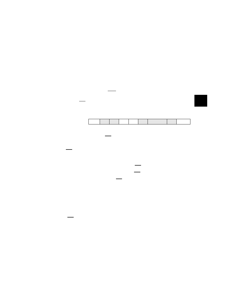
Address bit 7
bit 6
bit 5
bit 4
bit 3
bit 2
bit 1
bit 0
State
on reset
Miscellaneous Control Register
$0C
KBIE
KBIC
INTO
INTE LVRE
SM
IRQ2F IRQ2E 0001 0000
TPG
39
05SR3.Book Page 5 Thursday, August 4, 2005 1:08 PM
相关PDF资料 |
PDF描述 |
|---|---|
| VI-B5L-CU-F4 | CONVERTER MOD DC/DC 28V 200W |
| VI-B5L-CU-F1 | CONVERTER MOD DC/DC 28V 200W |
| MC68711E20MFNE2 | IC MCU 8BIT 52-PLCC |
| VI-B5K-CU-F2 | CONVERTER MOD DC/DC 40V 200W |
| VI-B5B-CU-F2 | CONVERTER MOD DC/DC 95V 200W |
相关代理商/技术参数 |
参数描述 |
|---|---|
| MC68HC706P6ACDW | 制造商:Motorola Inc 功能描述: |
| MC68HC708MP16CFU | 制造商:MAJOR 功能描述: |
| MC68HC711D3CFBE2 | 制造商:Freescale Semiconductor 功能描述: |
| MC68HC711D3CFN2 | 功能描述:IC MCU 2MHZ 4K OTP 44-PLCC RoHS:否 类别:集成电路 (IC) >> 嵌入式 - 微控制器, 系列:HC11 其它有关文件:STM32F101T8 View All Specifications 特色产品:STM32 32-bit Cortex MCUs 标准包装:490 系列:STM32 F1 核心处理器:ARM? Cortex?-M3 芯体尺寸:32-位 速度:36MHz 连通性:I²C,IrDA,LIN,SPI,UART/USART 外围设备:DMA,PDR,POR,PVD,PWM,温度传感器,WDT 输入/输出数:26 程序存储器容量:64KB(64K x 8) 程序存储器类型:闪存 EEPROM 大小:- RAM 容量:10K x 8 电压 - 电源 (Vcc/Vdd):2 V ~ 3.6 V 数据转换器:A/D 10x12b 振荡器型:内部 工作温度:-40°C ~ 85°C 封装/外壳:36-VFQFN,36-VFQFPN 包装:托盘 配用:497-10030-ND - STARTER KIT FOR STM32497-8853-ND - BOARD DEMO STM32 UNIV USB-UUSCIKSDKSTM32-PL-ND - KIT IAR KICKSTART STM32 CORTEXM3497-8512-ND - KIT STARTER FOR STM32F10XE MCU497-8505-ND - KIT STARTER FOR STM32F10XE MCU497-8304-ND - KIT STM32 MOTOR DRIVER BLDC497-6438-ND - BOARD EVALUTION FOR STM32 512K497-6289-ND - KIT PERFORMANCE STICK FOR STM32MCBSTM32UME-ND - BOARD EVAL MCBSTM32 + ULINK-MEMCBSTM32U-ND - BOARD EVAL MCBSTM32 + ULINK2更多... 其它名称:497-9032STM32F101T8U6-ND |
| MC68HC711D3CFNE2 | 功能描述:8位微控制器 -MCU 8B OTP 192RAM 2 MHZ RoHS:否 制造商:Silicon Labs 核心:8051 处理器系列:C8051F39x 数据总线宽度:8 bit 最大时钟频率:50 MHz 程序存储器大小:16 KB 数据 RAM 大小:1 KB 片上 ADC:Yes 工作电源电压:1.8 V to 3.6 V 工作温度范围:- 40 C to + 105 C 封装 / 箱体:QFN-20 安装风格:SMD/SMT |
发布紧急采购,3分钟左右您将得到回复。