- 您现在的位置:买卖IC网 > PDF目录4033 > MC7457RX1000NC (Freescale Semiconductor)IC MPU RISC 32BIT 483FCCBGA PDF资料下载
参数资料
| 型号: | MC7457RX1000NC |
| 厂商: | Freescale Semiconductor |
| 文件页数: | 16/71页 |
| 文件大小: | 0K |
| 描述: | IC MPU RISC 32BIT 483FCCBGA |
| 标准包装: | 36 |
| 系列: | MPC74xx |
| 处理器类型: | 32-位 MPC74xx PowerPC |
| 速度: | 1.0GHz |
| 电压: | 1.1V |
| 安装类型: | 表面贴装 |
| 封装/外壳: | 483-BCBGA,FCCBGA |
| 供应商设备封装: | 483-FCCBGA(29x29) |
| 包装: | 托盘 |
第1页第2页第3页第4页第5页第6页第7页第8页第9页第10页第11页第12页第13页第14页第15页当前第16页第17页第18页第19页第20页第21页第22页第23页第24页第25页第26页第27页第28页第29页第30页第31页第32页第33页第34页第35页第36页第37页第38页第39页第40页第41页第42页第43页第44页第45页第46页第47页第48页第49页第50页第51页第52页第53页第54页第55页第56页第57页第58页第59页第60页第61页第62页第63页第64页第65页第66页第67页第68页第69页第70页第71页
Electrical and Thermal Characteristics
MPC7457 RISC Microprocessor Hardware Specifications, Rev. 8
Freescale Semiconductor
23
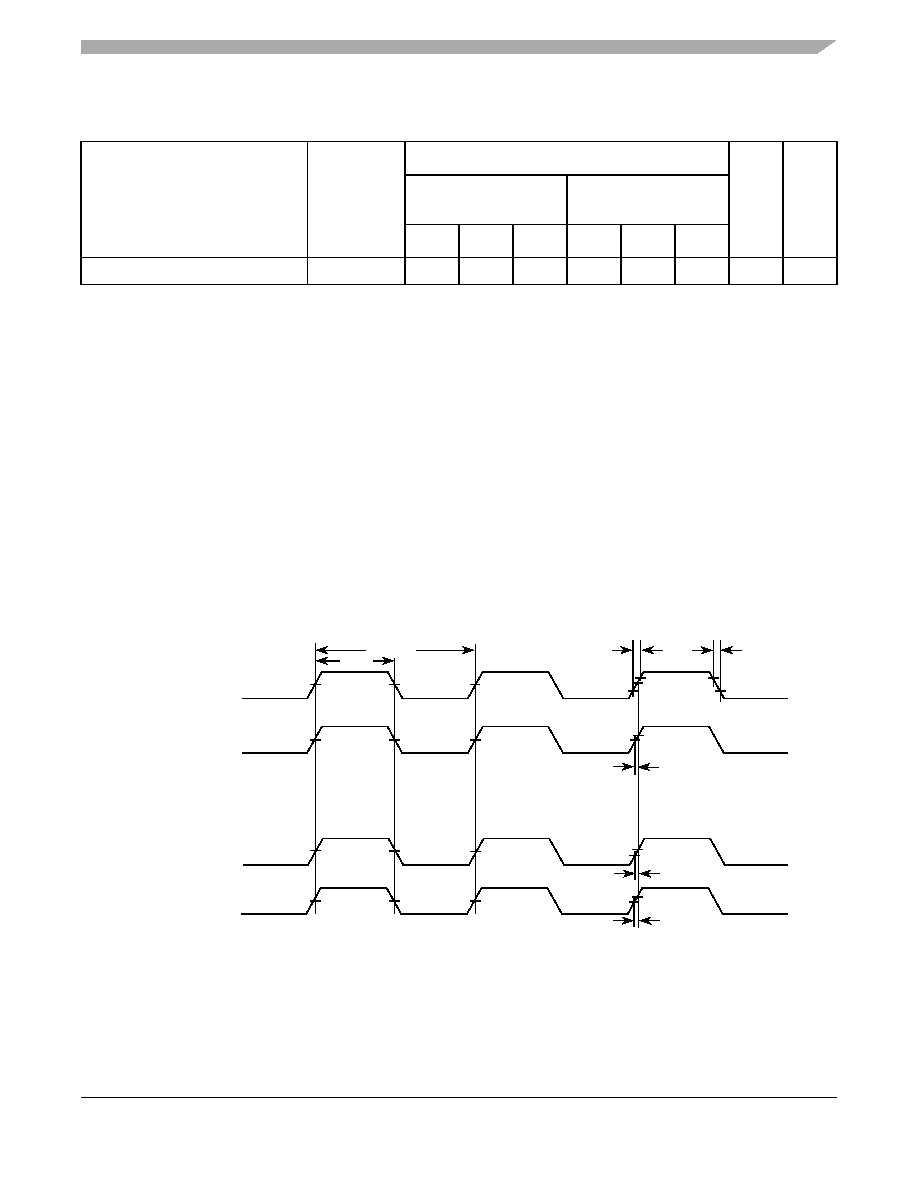
The L3_CLK timing diagram is shown in Figure 7.
Figure 7. L3_CLK_OUT Output Timing Diagram
L3 clock jitter
—
± 75
—
± 75
ps
5
Notes:
1. The maximum L3 clock frequency (and minimum L3 clock period) will be system dependent. See Section 5.2.3, “L3 Clock
AC Specifications,” for an explanation that this maximum frequency is not functionally tested at speed by Freescale. The
minimum L3 clock frequency and period are fSYSCLK and tSYSCLK, respectively.
2. The nominal duty cycle of the L3 output clocks is 50% measured at midpoint voltage.
3. Maximum possible skew between L3_CLK0 and L3_CLK1. This parameter is critical to the address and control signals which
are common to both SRAM chips in the L3.
4. Maximum possible skew between L3_CLK0 and L3_ECHO_CLK1 or between L3_CLK1 and L3_ECHO_CLK3 for PB2 or
Late Write SRAM. This parameter is critical to the read data signals because the processor uses the feedback loop to latch
data driven from the SRAM, each of which drives data based on L3_CLK0 or L3_CLK1.
5. Guaranteed by design and not tested. The input jitter on SYSCLK affects L3 output clocks and the L3 address, data, and
control signals equally and, therefore, is already comprehended in the AC timing and does not have to be considered in the
L3 timing analysis. The clock-to-clock jitter shown here is uncertainty in the internal clock period caused by supply voltage
noise or thermal effects. This is also comprehended in the AC timing specifications and need not be considered in the L3
timing analysis.
6. L3 I/O voltage mode must be configured by L3VSEL as described in Table 3, and voltage supplied at GVDD must match
mode selected as specified in Table 4. See Table 22 for revision level information and part marking.
Table 10. L3_CLK Output AC Timing Specifications (continued)
At recommended operating conditions. See Table 4.
Parameter
Symbol
Device Revision (L3 I/O Voltage) 6
Unit
Notes
Rev 1.1. (All I/O Modes)
Rev 1.2 (1.5-V I/O Mode)
Rev 1.2
(1.8-, 2.5-V I/O Modes)
Min
Typ
Max
Min
Typ
Max
L3_CLK0
VM
tL3CR
tL3CF
VM
L3_CLK1
VM
tL3_CLK
tCHCL
VM
L3_ECHO_CLK1
L3_ECHO_CLK3
VM
For PB2 or Late Write:
tL3CSKW1
tL3CSKW2
相关PDF资料 |
PDF描述 |
|---|---|
| IDT7025S30J | IC SRAM 128KBIT 30NS 84PLCC |
| XC4020XL-3HT144C | IC FPGA C-TEMP 3.3V 3SPD 144HQFP |
| XC4020XL-3BG256I | IC FPGA I-TEMP 3.3V 3SPD 256PBGA |
| XC4020XL-3BG256C | IC FPGA C-TEMP 3.3V 3SPD 256PBGA |
| IDT70V9269S9PRF8 | IC SRAM 256KBIT 9NS 128TQFP |
相关代理商/技术参数 |
参数描述 |
|---|---|
| MC7457RX1200PB | 制造商:Freescale Semiconductor 功能描述:A7, 1.35V +50MV/-30MV - Trays |
| MC7457RX1267LB | 制造商:Freescale Semiconductor 功能描述:MPC74XX RISC 32-BIT 0.13UM 1.267GHZ 1.5V/1.8V/2.5V 483-PIN F - Trays |
| MC7457RX1267LC | 功能描述:微处理器 - MPU APOLO7 RV1.2 1.3V 105C RoHS:否 制造商:Atmel 处理器系列:SAMA5D31 核心:ARM Cortex A5 数据总线宽度:32 bit 最大时钟频率:536 MHz 程序存储器大小:32 KB 数据 RAM 大小:128 KB 接口类型:CAN, Ethernet, LIN, SPI,TWI, UART, USB 工作电源电压:1.8 V to 3.3 V 最大工作温度:+ 85 C 安装风格:SMD/SMT 封装 / 箱体:FBGA-324 |
| MC7457RX1333PB | 制造商:Freescale Semiconductor 功能描述:A7, 1.35V +50MV/-30MV - Trays |
| MC7457RX733NC | 功能描述:IC MPU RISC 32BIT 483FCCBGA RoHS:否 类别:集成电路 (IC) >> 嵌入式 - 微处理器 系列:MPC74xx 标准包装:1 系列:MPC85xx 处理器类型:32-位 MPC85xx PowerQUICC III 特点:- 速度:1.2GHz 电压:1.1V 安装类型:表面贴装 封装/外壳:783-BBGA,FCBGA 供应商设备封装:783-FCPBGA(29x29) 包装:托盘 |
发布紧急采购,3分钟左右您将得到回复。