- 您现在的位置:买卖IC网 > PDF目录10940 > MC9328MX21CVK (Freescale Semiconductor)IC MCU I.MX21 266MHZ 289-MAPBGA PDF资料下载
参数资料
| 型号: | MC9328MX21CVK |
| 厂商: | Freescale Semiconductor |
| 文件页数: | 55/100页 |
| 文件大小: | 0K |
| 描述: | IC MCU I.MX21 266MHZ 289-MAPBGA |
| 标准包装: | 152 |
| 系列: | i.MX21 |
| 核心处理器: | ARM9 |
| 芯体尺寸: | 32-位 |
| 速度: | 266MHz |
| 连通性: | 1 线,EBI/EMI,I²C,IrDA,MMC,智能卡,SPI,SSI,UART/USART,USB OTG |
| 外围设备: | DMA,I²S,LCD,POR,PWM,WDT |
| 输入/输出数: | 192 |
| 程序存储器类型: | ROMless |
| 电压 - 电源 (Vcc/Vdd): | 1.45 V ~ 3.3 V |
| 振荡器型: | 外部 |
| 工作温度: | -40°C ~ 85°C |
| 封装/外壳: | 289-LFBGA |
| 包装: | 托盘 |
第1页第2页第3页第4页第5页第6页第7页第8页第9页第10页第11页第12页第13页第14页第15页第16页第17页第18页第19页第20页第21页第22页第23页第24页第25页第26页第27页第28页第29页第30页第31页第32页第33页第34页第35页第36页第37页第38页第39页第40页第41页第42页第43页第44页第45页第46页第47页第48页第49页第50页第51页第52页第53页第54页当前第55页第56页第57页第58页第59页第60页第61页第62页第63页第64页第65页第66页第67页第68页第69页第70页第71页第72页第73页第74页第75页第76页第77页第78页第79页第80页第81页第82页第83页第84页第85页第86页第87页第88页第89页第90页第91页第92页第93页第94页第95页第96页第97页第98页第99页第100页
MC9328MX21 Technical Data, Rev. 3.4
58
Freescale Semiconductor
Specifications
3.17
1-Wire Interface Timing
3.17.1
Reset Sequence with Reset Pulse Presence Pulse
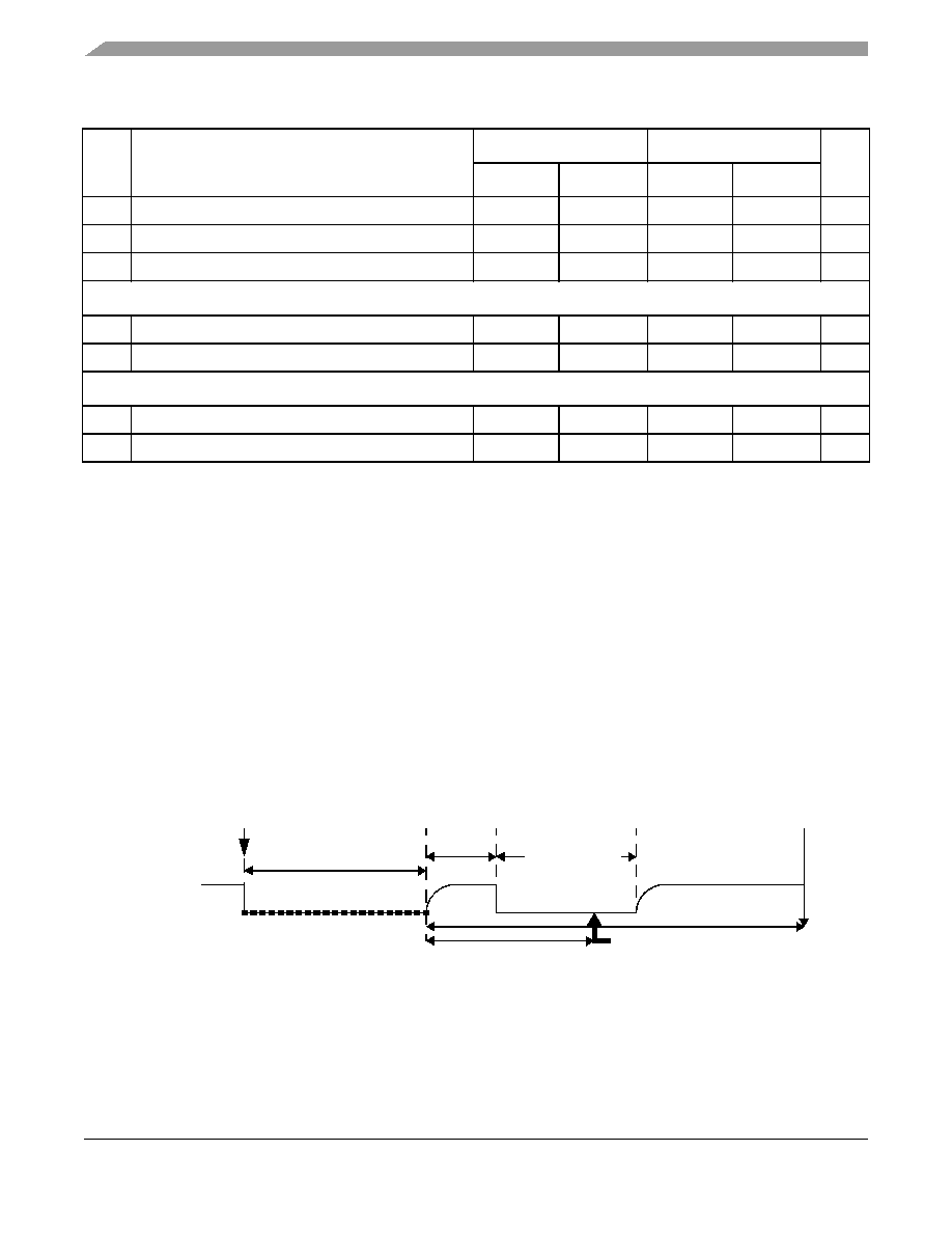
To begin any communications with the DS2502, it is required that an initialization procedure be issued. A
reset pulse must be generated and then a presence pulse must be detected. The minimum reset pulse length
is 480 us. The bus master (one-wire) will generate this pulse, then after the DS2502 detects a rising edge
on the one-wire bus, it will wait 15-60 us before it will transmit back a presence pulse. The presence pulse
will exist for 60-240 us.
The timing diagram for this sequence is shown in Figure 46.
Figure 46. 1-Wire Initialization
The reset pulse begins the initialization sequence and it is initiated when the RPP control register bit is set.
When the presence pulse is detected, this bit will be cleared. The presence pulse is used by the bus master
to determine if at least one DS2502 is connected. Software will determine if more than one DS2502 exists.
The one-wire will sample for the DS2502 presence pulse. The presence pulse is latched in the one-wire
28
(Tx) CK high to STXD high impedance
9.02
16.46
7.29
14.97
ns
29
SRXD setup time before (Rx) CK low
1.49
–
1.49
–
ns
30
SRXD hole time after (Rx) CK low
0
–
0
–
ns
Synchronous Internal Clock Operation (SSI3 Ports)
31
SRXD setup before (Tx) CK falling
21.99
–
21.99
–
ns
32
SRXD
h
old
a
fter
(
Tx)
C
K falling
0–0–
ns
Synchronous External Clock Operation (SSI3 Ports)
33
SRXD setup before (Tx) CK falling
3.80
–
3.80
–
ns
34
SRXD
h
old
a
fter
(
Tx)
C
K falling
0–0–
ns
1. All the timings for the SSI are given for a non-inverted serial clock polarity (TSCKP/RSCKP = 0) and a non-inverted frame sync
(TFSI/RFSI = 0). If the polarity of the clock and/or the frame sync have been inverted, all the timing remains valid by inverting
the clock signal STCK/SRCK and/or the frame sync STFS/SRFS shown in the tables and in the figures.
Table 37. SSI to SSI3 Ports Timing Parameters (Continued)
Ref
No.
Parameter
1.8 V
± 0.1 V
3.0 V
± 0.3 V
Unit
Minimum
Maximum
Minimum
Maximum
one-wire
DS2502
waits
15-60us
DS2502 Tx
“presence pulse”
60-240us
68us
BUS
Reset and Presence Pulses
One-Wire samples (set PST)
512us
AutoClear RPP
Control Bit
Set RPP
511 us
相关PDF资料 |
PDF描述 |
|---|---|
| VI-26N-CU-S | CONVERTER MOD DC/DC 18.5V 200W |
| AD74111YRUZ-REEL | IC CODEC AUDIO MONO LP 16TSSOP |
| VI-B23-IW-B1 | CONVERTER MOD DC/DC 24V 100W |
| VI-J3W-IX-S | CONVERTER MOD DC/DC 5.5V 75W |
| SSM2603CPZ-REEL7 | IC CODEC AUDIO LOW POWER 28LFCSP |
相关代理商/技术参数 |
参数描述 |
|---|---|
| MC9328MX21CVK | 制造商:Freescale Semiconductor 功能描述:Microcontroller |
| MC9328MX21CVKR2 | 功能描述:处理器 - 专门应用 DB I.MX21 PB-FR RoHS:否 制造商:Freescale Semiconductor 类型:Multimedia Applications 核心:ARM Cortex A9 处理器系列:i.MX6 数据总线宽度:32 bit 最大时钟频率:1 GHz 指令/数据缓存: 数据 RAM 大小:128 KB 数据 ROM 大小: 工作电源电压: 最大工作温度:+ 95 C 安装风格:SMD/SMT 封装 / 箱体:MAPBGA-432 |
| MC9328MX21CVM | 功能描述:处理器 - 专门应用 DB I.MX21 17X17 PB-FR RoHS:否 制造商:Freescale Semiconductor 类型:Multimedia Applications 核心:ARM Cortex A9 处理器系列:i.MX6 数据总线宽度:32 bit 最大时钟频率:1 GHz 指令/数据缓存: 数据 RAM 大小:128 KB 数据 ROM 大小: 工作电源电压: 最大工作温度:+ 95 C 安装风格:SMD/SMT 封装 / 箱体:MAPBGA-432 |
| MC9328MX21CVM | 制造商:Freescale Semiconductor 功能描述:Microprocessor |
| MC9328MX21CVMR2 | 功能描述:处理器 - 专门应用 DB I.MX21 17X17 PB-FR RoHS:否 制造商:Freescale Semiconductor 类型:Multimedia Applications 核心:ARM Cortex A9 处理器系列:i.MX6 数据总线宽度:32 bit 最大时钟频率:1 GHz 指令/数据缓存: 数据 RAM 大小:128 KB 数据 ROM 大小: 工作电源电压: 最大工作温度:+ 95 C 安装风格:SMD/SMT 封装 / 箱体:MAPBGA-432 |
发布紧急采购,3分钟左右您将得到回复。