- 您现在的位置:买卖IC网 > PDF目录45285 > MC9328MXLVH15 (MOTOROLA INC) 32-BIT, 150 MHz, RISC PROCESSOR, PBGA256 PDF资料下载
参数资料
| 型号: | MC9328MXLVH15 |
| 厂商: | MOTOROLA INC |
| 元件分类: | 微控制器/微处理器 |
| 英文描述: | 32-BIT, 150 MHz, RISC PROCESSOR, PBGA256 |
| 封装: | 14 X 14 MM, 1.30 MM HEIGHT, 0.80 MM PITCH, MAPBGA-256 |
| 文件页数: | 55/89页 |
| 文件大小: | 1869K |
| 代理商: | MC9328MXLVH15 |
第1页第2页第3页第4页第5页第6页第7页第8页第9页第10页第11页第12页第13页第14页第15页第16页第17页第18页第19页第20页第21页第22页第23页第24页第25页第26页第27页第28页第29页第30页第31页第32页第33页第34页第35页第36页第37页第38页第39页第40页第41页第42页第43页第44页第45页第46页第47页第48页第49页第50页第51页第52页第53页第54页当前第55页第56页第57页第58页第59页第60页第61页第62页第63页第64页第65页第66页第67页第68页第69页第70页第71页第72页第73页第74页第75页第76页第77页第78页第79页第80页第81页第82页第83页第84页第85页第86页第87页第88页第89页
Specifications
MOTOROLA
MC9328MXL Advance Information
59
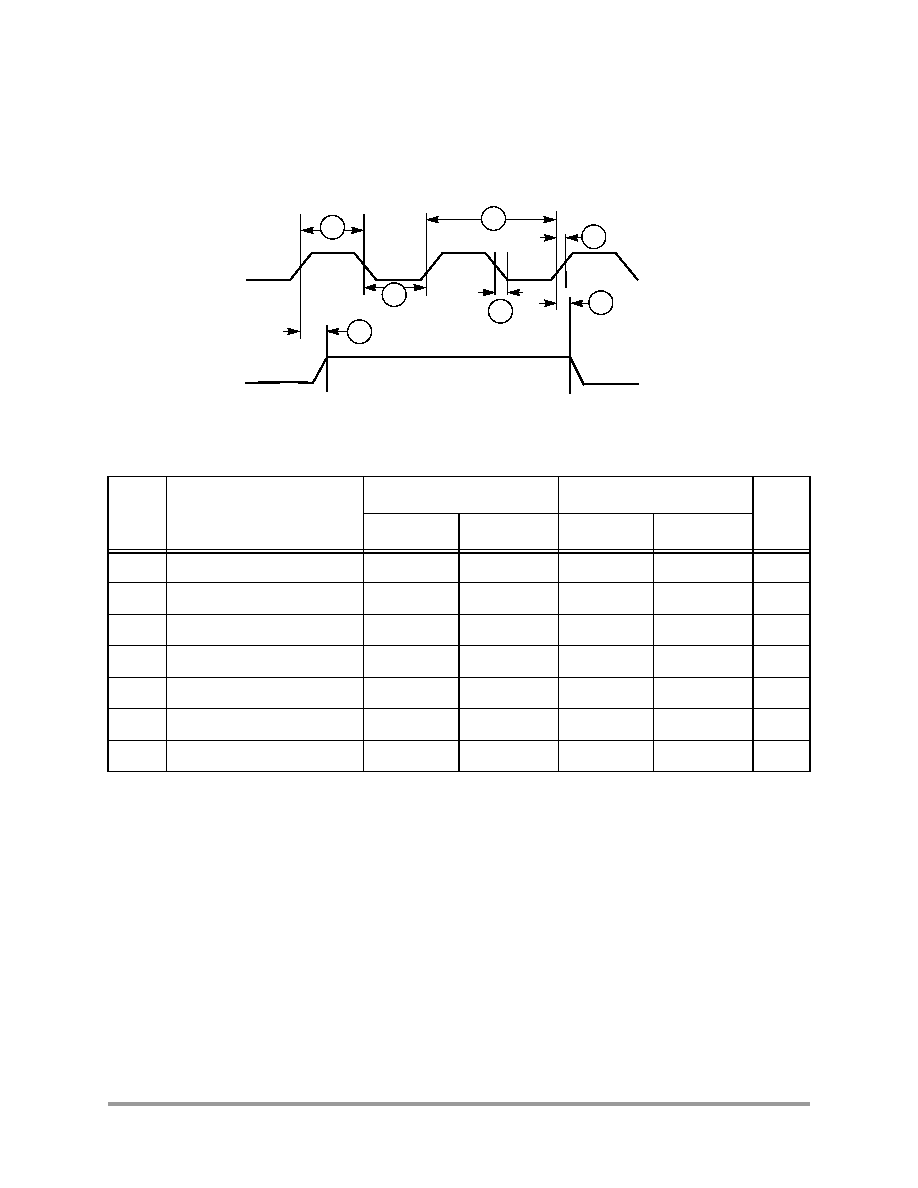
3.13 Pulse-Width Modulator
The PWM can be programmed to select one of two clock signals as its source frequency. The selected
clock signal is passed through a divider and a prescaler before being input to the counter. The output is
available at the pulse-width modulator output (PWMO) external pin. Its timing diagram is shown in
Figure 47. PWM Output Timing Diagram
3.14 SDRAM Controller
A write to an address within the memory region initiates the program sequence. The first command issued
to the SyncFlash is Load Command Register. The value in A [7:0] determines which operation the
command performs. For this write setup operation, an address of 0x40 is hardware generated. The bank
and other address lines are driven with the address to be programmed. The next command is Active which
registers the row address and confirms the bank address. The third command supplies the column address,
re-confirms the bank address, and supplies the data to be written. SyncFlash does not support burst writes,
therefore a Burst Terminate command is not required.
A read to the memory region initiates the status read sequence. The first command issued to the SyncFlash
is the Load Command Register with A [7:0] set to 0x70 which corresponds to the Read Status Register
operation. The bank and other address lines are driven to the selected address. The second command is
Table 21. PWM Output Timing Parameter Table
Ref
No.
Parameter
1.8V ± 0.10V
3.0V ± 0.30V
Unit
Minimum
Maximum
Minimum
Maximum
1
System CLK frequency1
1.
CL of PWMO = 30 pF
0870
100
MHz
2a
Clock high time1
3.3
—
5/10
—
ns
2b
Clock low time1
7.5
—
5/10
—
ns
3a
Clock fall time1
—5—
5/10
ns
3b
Clock rise time1
—
6.67
—
5/10
ns
4a
Output delay time1
5.7
—
5
—
ns
4b
Output setup time1
5.7
—
5
—
ns
System Clock
2a
1
PWM Output
3b
2b
3a
4b
4a
相关PDF资料 |
PDF描述 |
|---|---|
| MC9328MXLDVP15 | 150 MHz, RISC PROCESSOR, PBGA225 |
| MC9328MXLDVF15 | 150 MHz, RISC PROCESSOR, PBGA225 |
| MC9328MXLVF15 | 32-BIT, 150 MHz, RISC PROCESSOR, PBGA225 |
| MC9328MXLVH20 | 32-BIT, 200 MHz, RISC PROCESSOR, PBGA256 |
| MC9328MXLDVM20 | 200 MHz, RISC PROCESSOR, PBGA256 |
相关代理商/技术参数 |
参数描述 |
|---|---|
| MC9328MXLVH20 | 制造商:FREESCALE 制造商全称:Freescale Semiconductor, Inc 功能描述:i.MX Integrated Portable System Processor |
| MC9328MXLVH20R2 | 制造商:Rochester Electronics LLC 功能描述:DRAGONBALL CORSICA - Bulk 制造商:Motorola Inc 功能描述: |
| MC9328MXLVM15 | 功能描述:处理器 - 专门应用 DRAGONBALL CORSICA PB-FR RoHS:否 制造商:Freescale Semiconductor 类型:Multimedia Applications 核心:ARM Cortex A9 处理器系列:i.MX6 数据总线宽度:32 bit 最大时钟频率:1 GHz 指令/数据缓存: 数据 RAM 大小:128 KB 数据 ROM 大小: 工作电源电压: 最大工作温度:+ 95 C 安装风格:SMD/SMT 封装 / 箱体:MAPBGA-432 |
| MC9328MXLVM15R2 | 功能描述:处理器 - 专门应用 DRAGONBALL CORSICA PB-FR RoHS:否 制造商:Freescale Semiconductor 类型:Multimedia Applications 核心:ARM Cortex A9 处理器系列:i.MX6 数据总线宽度:32 bit 最大时钟频率:1 GHz 指令/数据缓存: 数据 RAM 大小:128 KB 数据 ROM 大小: 工作电源电压: 最大工作温度:+ 95 C 安装风格:SMD/SMT 封装 / 箱体:MAPBGA-432 |
| MC9328MXLVM20 | 功能描述:处理器 - 专门应用 DRAGONBALL CORSICA PB-FR RoHS:否 制造商:Freescale Semiconductor 类型:Multimedia Applications 核心:ARM Cortex A9 处理器系列:i.MX6 数据总线宽度:32 bit 最大时钟频率:1 GHz 指令/数据缓存: 数据 RAM 大小:128 KB 数据 ROM 大小: 工作电源电压: 最大工作温度:+ 95 C 安装风格:SMD/SMT 封装 / 箱体:MAPBGA-432 |
发布紧急采购,3分钟左右您将得到回复。