- 您现在的位置:买卖IC网 > PDF目录11784 > MCZ33780EG (Freescale Semiconductor)IC MASTER DUAL DBUS DIFF 16-SOIC PDF资料下载
参数资料
| 型号: | MCZ33780EG |
| 厂商: | Freescale Semiconductor |
| 文件页数: | 18/37页 |
| 文件大小: | 0K |
| 描述: | IC MASTER DUAL DBUS DIFF 16-SOIC |
| 标准包装: | 47 |
| 系列: | * |
| 应用: | * |
| 接口: | * |
| 电源电压: | * |
| 封装/外壳: | 16-SOIC(0.295",7.50mm 宽) |
| 供应商设备封装: | 16-SOIC W |
| 包装: | 管件 |
| 安装类型: | 表面贴装 |
| 产品目录页面: | 808 (CN2011-ZH PDF) |
第1页第2页第3页第4页第5页第6页第7页第8页第9页第10页第11页第12页第13页第14页第15页第16页第17页当前第18页第19页第20页第21页第22页第23页第24页第25页第26页第27页第28页第29页第30页第31页第32页第33页第34页第35页第36页第37页
Analog Integrated Circuit Device Data
Freescale Semiconductor
25
33780
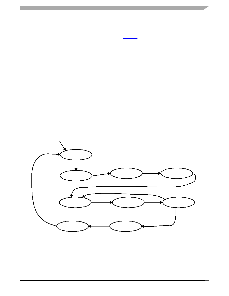
FUNCTIONAL DEVICE OPERATION
LOGIC COMMANDS AND REGISTERS
When enable is true and there is at least one valid entry in
the transmit FIFO, the DBUS frame signal is driven low to
start a frame. States WAIT_SIG_DLY_0 through
WAIT_SIG_DLY_2 create a one DBUS bit-time delay before
the start of the first data bit. After WAIT_SIG_DLY_2, the
DBUS_BIT_PTR gets initialized to the total word length, as
determined by the MSx, SWLENx, and CRCLENx bits. The
XFER_DBUS_BIT_0 state is then entered.
XFER_DBUS_BIT_0 through XFER_DBUS_BIT_2 form a
loop where each pass corresponds to one DBUS bit time.
During the first third of the bit the DSIxS signal is low, during
the second third DSIxS is low for a zero or high for a one,
during the last third of the bit time DSIxS is high. Provided this
is not the end of the last CRC bit, the bit pointer is
decremented and the loop is repeated.
After the last CRC bit, the DBUS_R_PUSH state is
entered. This state ensures that the CRC flag is stable prior
to adjusting the receive (and transmit) FIFO pointers. The
DBUS_X_POP state prevents an X_FIFO_POP from
occurring at the same time as an R_FIFO_PUSH.
After DBUS_X_POP, the state transitions back to the
WAIT_FRAME_DLY state. This state ensures proper frame
spacing is allowed to charge up the storage capacitors in
remote nodes. Notice that the delay counter was reset at the
end of the last CRC bit so the delay period can start to time
out even while the DBUS_R_PUSH and DBUS_X_POP
states are being processed.
Figure 22 describes the operation of the transmit FIFO.
This FIFO is four levels deep, including the stage which is
written into by the SPI and the stage which provides the data
for the current DBUS serial transfer. State transitions in this
state machine occur at the trailing edges of X_FIFO_PUSH
and X_FIFO_POP.
When this FIFO is completely empty, the SPI can write
four new values to fill the FIFO without waiting for any action
on the DBUS side of the FIFO. Values are pushed into the
FIFO from the SPI interface and values are popped after they
have been serially sent out of the DBUS interface. When the
FIFO is full, additional attempts to write new data from the
SPI side are ignored (the host MCU should be sure the
TFNFx status bit is set before writing more data to the FIFO).
Reset, abort, or enable going to zero causes
asynchronous entry to the TX_IDLE state, which
corresponds to the FIFO empty condition. The push and pop
pointers are cleared and X_FIFO_EMPTY is set to true.
X_FIFO_PUSH causes the push pointer to be incremental,
X_FIFO_EMPTY to be set to false, and the state to transition
to TX_NOT_EMPTY. The push request comes from the SPI
transfer state machine after a new value has been written into
the FIFO.
Figure 21. State Diagram of DBUS Transfer
STATE TRANSISITONS OCCUR
ON POS EDGE OF SCALED
DBUS 1/3RD BIT CLOCK
WAIT_FRAME_DLY
WAIT_SIG_DLY_0
WAIT_SIG_DLY_1
WAIT_SIG_DLY_2
XFER_DBUS_BIT_0
XFER_DBUS_BIT_1
XFER_DEBUS_BIT_2
DBUS_X_POP
DBUS_R_PUSH
R_FIFO_PUSH = 0;
X_FIFO_POP = 0;
DSIS = DATA;
DSIS = 1;
DELAY_OVER &
X_FIFO_NOT_EMPTY/
DSIF = 0;
WAIT_SIG_DLY[0..2] CAUSES 1 BIT-TIME DLY TO 1ST BIT FALLING EDGE
~LAST_CRC_BIT/
DBUS_BIT_PTR = DBUS_BIT_PTR-1;
DSIS = 0;
LAST_CRC-BIT/
DSIF = 1, DSIS = 1;
RESET DELAY_CNR;
R_FIFO_PUSH = 1
X_FIFO_POP = 1;
DBUS_BIT_PTR = 8 to 15, OR 23;
DSIS = 0;
RSTB ACTIVE or ABORT or ~EN/
DSIF = 1, DSIS = 1;
RESET_DELAY_CNTR;
相关PDF资料 |
PDF描述 |
|---|---|
| MC33972ATEW | IC SWITCH DETECT SPI 32-SOIC |
| VI-J5P-IW-F4 | CONVERTER MOD DC/DC 13.8V 100W |
| VI-J5P-IW-F2 | CONVERTER MOD DC/DC 13.8V 100W |
| MCZ33905BD5EK | IC SBC CAN HS 5.0V 54SOIC |
| NCN8024DWR2G | IC SMART CARD IC2 28SOIC |
相关代理商/技术参数 |
参数描述 |
|---|---|
| MCZ33780EG | 制造商:Freescale Semiconductor 功能描述:DUAL DBUS MASTER INTERFACE 16SOIC |
| MCZ33780EGR2 | 功能描述:多路器开关 IC DBUS MASTER RoHS:否 制造商:Texas Instruments 通道数量:1 开关数量:4 开启电阻(最大值):7 Ohms 开启时间(最大值): 关闭时间(最大值): 传播延迟时间:0.25 ns 工作电源电压:2.3 V to 3.6 V 工作电源电流: 最大工作温度:+ 85 C 安装风格:SMD/SMT 封装 / 箱体:UQFN-16 |
| MCZ33781EK | 功能描述:输入/输出控制器接口集成电路 DBUS2 MASTER STND RoHS:否 制造商:Silicon Labs 产品: 输入/输出端数量: 工作电源电压: 最大工作温度:+ 85 C 最小工作温度:- 40 C 安装风格:SMD/SMT 封装 / 箱体:QFN-64 封装:Tray |
| MCZ33781EKR2 | 功能描述:输入/输出控制器接口集成电路 DBUS2 MASTER STND RoHS:否 制造商:Silicon Labs 产品: 输入/输出端数量: 工作电源电压: 最大工作温度:+ 85 C 最小工作温度:- 40 C 安装风格:SMD/SMT 封装 / 箱体:QFN-64 封装:Tray |
| MCZ33784EF | 功能描述:加速计 - 板上安装 DBUS2 SENSOR INTERFACE RoHS:否 制造商:Murata 传感轴:Double 加速:12 g 灵敏度: 封装 / 箱体: 输出类型:Analog 数字输出 - 位数:11 bit 电源电压-最大:5.25 V 电源电压-最小:4.75 V 电源电流:4 mA 最大工作温度:+ 125 C 最小工作温度:- 40 C |
发布紧急采购,3分钟左右您将得到回复。