- 您现在的位置:买卖IC网 > PDF目录11784 > MCZ33780EG (Freescale Semiconductor)IC MASTER DUAL DBUS DIFF 16-SOIC PDF资料下载
参数资料
| 型号: | MCZ33780EG |
| 厂商: | Freescale Semiconductor |
| 文件页数: | 7/37页 |
| 文件大小: | 0K |
| 描述: | IC MASTER DUAL DBUS DIFF 16-SOIC |
| 标准包装: | 47 |
| 系列: | * |
| 应用: | * |
| 接口: | * |
| 电源电压: | * |
| 封装/外壳: | 16-SOIC(0.295",7.50mm 宽) |
| 供应商设备封装: | 16-SOIC W |
| 包装: | 管件 |
| 安装类型: | 表面贴装 |
| 产品目录页面: | 808 (CN2011-ZH PDF) |
第1页第2页第3页第4页第5页第6页当前第7页第8页第9页第10页第11页第12页第13页第14页第15页第16页第17页第18页第19页第20页第21页第22页第23页第24页第25页第26页第27页第28页第29页第30页第31页第32页第33页第34页第35页第36页第37页
Analog Integrated Circuit Device Data
Freescale Semiconductor
15
33780
FUNCTIONAL DESCRIPTIONS
FUNCTIONAL INTERNAL BLOCK DESCRIPTION
PROTOCOL ENGINE
This block converts the data to be transmitted from the
registers into the DBUS sequences, and converts DBUS
response sequences to data in the registers. It generates the
proper DBUS timing.
The DBUS transmit protocol uses a return to 1 type data
with a duty cycle determined by the logic state. The protocol
requires Cyclical Redundancy Check (CRC) generation and
validation.
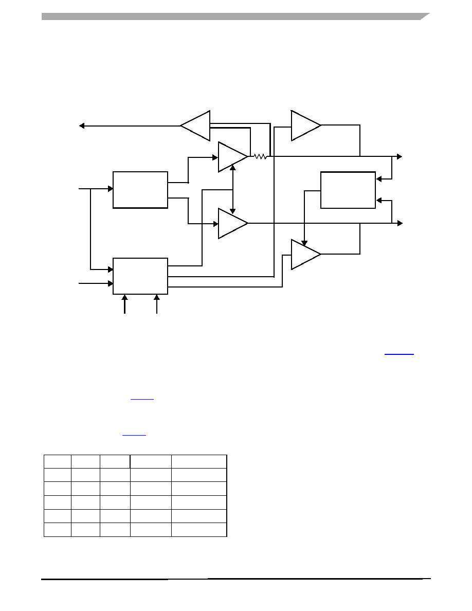
Figure 10. Driver/Receiver Block Diagram
DBUS DRIVER /RECEIVER (PHYSICAL LAYER)
This block translates the transmit data to the voltage and
current needed to drive the DBUS. It also detects the
response current from the slave devices and translates that
current into digital levels. These circuits can drive their
outputs to the levels listed in Table 5.
The internal signal DSIF controls the Idle to Signalling
state change, and internal signal DSIS controls the signal
level, high or low. DSIR is the slave device response signal to
the logic. This is shown in Table 6.
The DBUS driver block diagram is shown in Figure 10. The
circuit uses independent drivers for the Idle and Signal states.
This allows each driver to be optimized for its function. The
Idle driver is active in Idle and during the transitions from Idle
to Signal high and Signal high to Idle. The Signal driver is only
active during actual signaling. Both drivers are disabled in
HiZ.
The Idle driver is required to supply a high current to
recharge the Slave device storage capacitors. It is also
required to drive the DBUS load capacitances and control the
slew rate over a wide supply voltage range. The DnH and
DnL Idle drivers are each optimized for their specific drive
requirements.
The Signal driver is optimized for driving the DBUS load,
and has the requirement of good slew rate control and
stability over a wide range of load conditions. The DnH and
DnL outputs use identical Signal driver circuits.
To ensure stability of the Signal driver, capacitors must be
connected between each output and ground. These are the
DBUS common mode capacitors. In addition, a bypass
capacitor is required at VSUP. These capacitors must be
located close to the IC pins and provide a low impedance
path to ground.
DnH
DnL
Differential
Control
DSIR
DSIS
DSIF
Common
Overvoltage TLIM
Signal
Generation
Mode
Correction
Signal
Idle
Comp.
Table 6. Internal Signal Truth Table
DSIF
DSIS
TLIM
DSIR
DnD
0
Return Data
Signal Low
0
1
0
Return Data
Signal High
1
0
High Impedance
1
0
Idle
X
1
0
High Impedance
相关PDF资料 |
PDF描述 |
|---|---|
| MC33972ATEW | IC SWITCH DETECT SPI 32-SOIC |
| VI-J5P-IW-F4 | CONVERTER MOD DC/DC 13.8V 100W |
| VI-J5P-IW-F2 | CONVERTER MOD DC/DC 13.8V 100W |
| MCZ33905BD5EK | IC SBC CAN HS 5.0V 54SOIC |
| NCN8024DWR2G | IC SMART CARD IC2 28SOIC |
相关代理商/技术参数 |
参数描述 |
|---|---|
| MCZ33780EG | 制造商:Freescale Semiconductor 功能描述:DUAL DBUS MASTER INTERFACE 16SOIC |
| MCZ33780EGR2 | 功能描述:多路器开关 IC DBUS MASTER RoHS:否 制造商:Texas Instruments 通道数量:1 开关数量:4 开启电阻(最大值):7 Ohms 开启时间(最大值): 关闭时间(最大值): 传播延迟时间:0.25 ns 工作电源电压:2.3 V to 3.6 V 工作电源电流: 最大工作温度:+ 85 C 安装风格:SMD/SMT 封装 / 箱体:UQFN-16 |
| MCZ33781EK | 功能描述:输入/输出控制器接口集成电路 DBUS2 MASTER STND RoHS:否 制造商:Silicon Labs 产品: 输入/输出端数量: 工作电源电压: 最大工作温度:+ 85 C 最小工作温度:- 40 C 安装风格:SMD/SMT 封装 / 箱体:QFN-64 封装:Tray |
| MCZ33781EKR2 | 功能描述:输入/输出控制器接口集成电路 DBUS2 MASTER STND RoHS:否 制造商:Silicon Labs 产品: 输入/输出端数量: 工作电源电压: 最大工作温度:+ 85 C 最小工作温度:- 40 C 安装风格:SMD/SMT 封装 / 箱体:QFN-64 封装:Tray |
| MCZ33784EF | 功能描述:加速计 - 板上安装 DBUS2 SENSOR INTERFACE RoHS:否 制造商:Murata 传感轴:Double 加速:12 g 灵敏度: 封装 / 箱体: 输出类型:Analog 数字输出 - 位数:11 bit 电源电压-最大:5.25 V 电源电压-最小:4.75 V 电源电流:4 mA 最大工作温度:+ 125 C 最小工作温度:- 40 C |
发布紧急采购,3分钟左右您将得到回复。