- 您现在的位置:买卖IC网 > PDF目录11784 > MCZ33780EG (Freescale Semiconductor)IC MASTER DUAL DBUS DIFF 16-SOIC PDF资料下载
参数资料
| 型号: | MCZ33780EG |
| 厂商: | Freescale Semiconductor |
| 文件页数: | 9/37页 |
| 文件大小: | 0K |
| 描述: | IC MASTER DUAL DBUS DIFF 16-SOIC |
| 标准包装: | 47 |
| 系列: | * |
| 应用: | * |
| 接口: | * |
| 电源电压: | * |
| 封装/外壳: | 16-SOIC(0.295",7.50mm 宽) |
| 供应商设备封装: | 16-SOIC W |
| 包装: | 管件 |
| 安装类型: | 表面贴装 |
| 产品目录页面: | 808 (CN2011-ZH PDF) |
第1页第2页第3页第4页第5页第6页第7页第8页当前第9页第10页第11页第12页第13页第14页第15页第16页第17页第18页第19页第20页第21页第22页第23页第24页第25页第26页第27页第28页第29页第30页第31页第32页第33页第34页第35页第36页第37页
Analog Integrated Circuit Device Data
Freescale Semiconductor
17
33780
FUNCTIONAL DESCRIPTIONS
FUNCTIONAL INTERNAL BLOCK DESCRIPTION
SPREAD SPECTRUM
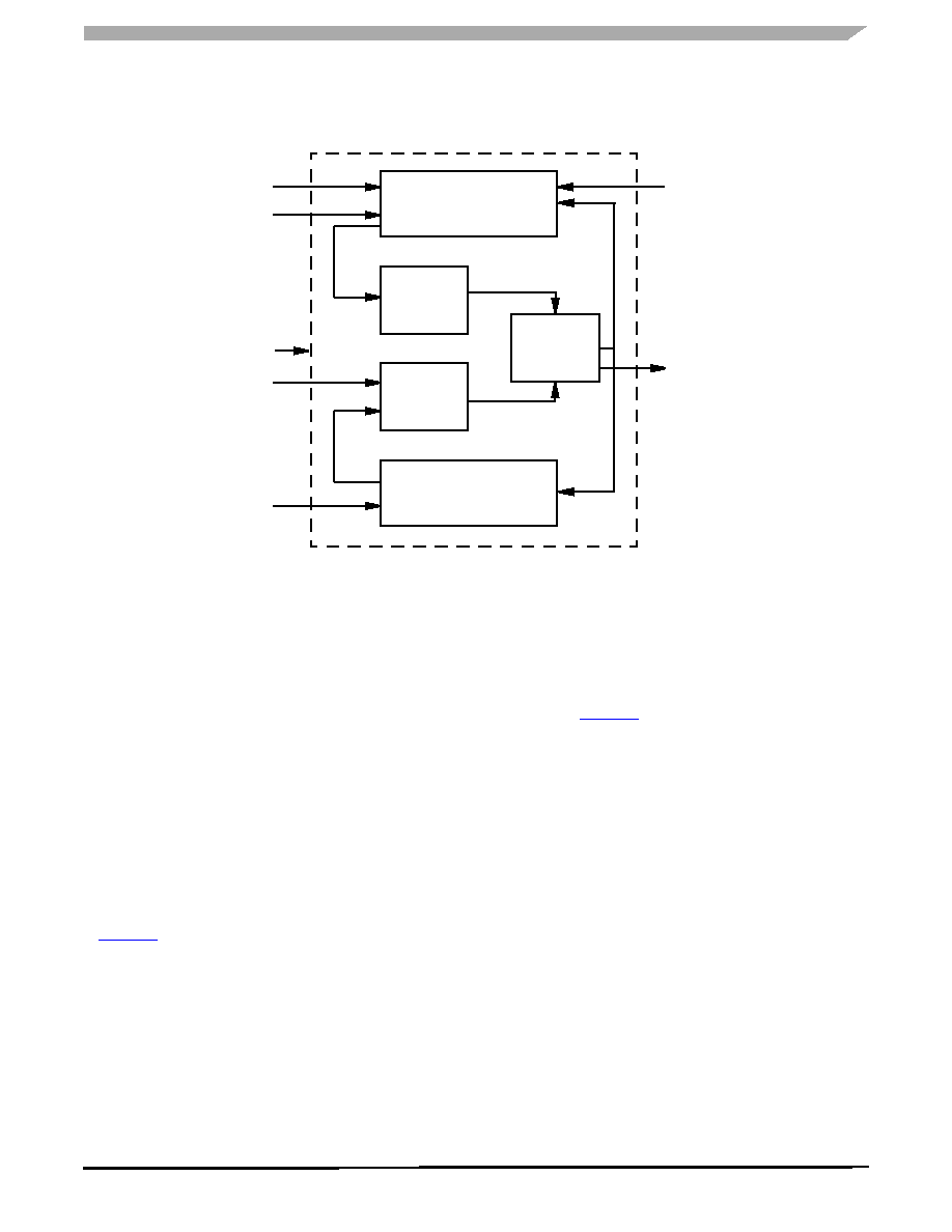
Figure 12. Spread Spectrum Block Diagram
The dominant source of radiated electromagnetic
interference (EMI) from the DBUS bus is due to the regular
periodic frequency of the data bits. At a steady bit rate, the
time period for each bit is the same, which results in a steady
fundamental frequency plus harmonics. This results in
undesired signals appearing at multiples of the frequency
that can be strong enough to interfere with a desired signal.
A significant decrease of radiated EMI can be achieved by
randomly changing the duration of each bit. This can
significantly reduce the amplitude by having the signal spend
a much smaller percentage of time at any specific frequency.
The signal strength of the fundamental and harmonics are
reduced directly by the percentage of time it spends on a
specific frequency. For instance, if the bit rate is 136 kbps,
there will be a harmonic at 680 kHz. If it is changed in
frequency so that only 1/10 of the bits are at the 136 kbps
rate, the signal energy at 680 kHz will be reduced by 90%.
A circuit to do this is included in this IC and can perform the
spreading of the signal independently for each channel. This
is done in the Spread Spectrum (SS) Block Diagram shown
in Figure 12.
Spreading can be enabled by setting the SSENn bits in the
DnSSCTRL registers. There are 64 possible bit durations that
are equally spaced between the shortest and longest bit
times. Because they are evenly spaced by a time difference
and not by a frequency difference (the reciprocal of time), all
frequency domain parameters of the SS block are expressed
in units of time.
VCO
The output of the voltage-controlled oscillator (VCO) is
used as the bit rate clock. Three cycles of this clock are used
to create each bit of data on the DBUS.
There are two voltages that control the period (1/
frequency) of the signal coming from the VCO. The voltage
coming from the Center Frequency DAC (Digital-to-Analog
Converter) in Figure 12 is used to keep the average period
constant. The voltage coming from the Spreader DAC
changes the period in random steps to spread the signal. The
Phase Locked Loop (PLL)-derived changes are much slower
to update the period than the ones derived from the Spreader
Logic. This prevents the two “loops” from interacting with
each other.
PLL
The PLL loop compensates for temperature drift and the
variations in processing of the IC that would otherwise
change the average data rate (center frequency). It does this
by comparing a time reference derived from the clock signal
(4.0 MHz) to the period of the VCO output. If the ratio is not
correct, it will change the frequency of the VCO by changing
the digital value it sends to the Center Frequency DAC.
The PLL has fast and slow update rates for making these
changes. It enters a fast update mode automatically anytime
the OFFSET register is written to using the SPI, or following
a reset. This fast acquisition mode consists of 64 VCO update
cycles (1.4 ms per update cycle) that last about 90 ms. This
is done to quickly adjust the center frequency after changes
have been made. After the fast acquisition, the PLL switches
PLL Logic
Spreader Logic
Center
Frequency
DAC
Modulation
DAC
VCO
CLK (4.0 MHz typ)
CLK_VCOn (408 kHz typ)
OFFSET[8:0]
PLLOFF
SSEN
DEV[1:0]
PRBS[1:0]
SSUD
相关PDF资料 |
PDF描述 |
|---|---|
| MC33972ATEW | IC SWITCH DETECT SPI 32-SOIC |
| VI-J5P-IW-F4 | CONVERTER MOD DC/DC 13.8V 100W |
| VI-J5P-IW-F2 | CONVERTER MOD DC/DC 13.8V 100W |
| MCZ33905BD5EK | IC SBC CAN HS 5.0V 54SOIC |
| NCN8024DWR2G | IC SMART CARD IC2 28SOIC |
相关代理商/技术参数 |
参数描述 |
|---|---|
| MCZ33780EG | 制造商:Freescale Semiconductor 功能描述:DUAL DBUS MASTER INTERFACE 16SOIC |
| MCZ33780EGR2 | 功能描述:多路器开关 IC DBUS MASTER RoHS:否 制造商:Texas Instruments 通道数量:1 开关数量:4 开启电阻(最大值):7 Ohms 开启时间(最大值): 关闭时间(最大值): 传播延迟时间:0.25 ns 工作电源电压:2.3 V to 3.6 V 工作电源电流: 最大工作温度:+ 85 C 安装风格:SMD/SMT 封装 / 箱体:UQFN-16 |
| MCZ33781EK | 功能描述:输入/输出控制器接口集成电路 DBUS2 MASTER STND RoHS:否 制造商:Silicon Labs 产品: 输入/输出端数量: 工作电源电压: 最大工作温度:+ 85 C 最小工作温度:- 40 C 安装风格:SMD/SMT 封装 / 箱体:QFN-64 封装:Tray |
| MCZ33781EKR2 | 功能描述:输入/输出控制器接口集成电路 DBUS2 MASTER STND RoHS:否 制造商:Silicon Labs 产品: 输入/输出端数量: 工作电源电压: 最大工作温度:+ 85 C 最小工作温度:- 40 C 安装风格:SMD/SMT 封装 / 箱体:QFN-64 封装:Tray |
| MCZ33784EF | 功能描述:加速计 - 板上安装 DBUS2 SENSOR INTERFACE RoHS:否 制造商:Murata 传感轴:Double 加速:12 g 灵敏度: 封装 / 箱体: 输出类型:Analog 数字输出 - 位数:11 bit 电源电压-最大:5.25 V 电源电压-最小:4.75 V 电源电流:4 mA 最大工作温度:+ 125 C 最小工作温度:- 40 C |
发布紧急采购,3分钟左右您将得到回复。