- 您现在的位置:买卖IC网 > PDF目录379321 > MJE16106 (MOTOROLA INC) POWER TRANSISTORS 8 AMPERES 400 VOLTS 100 AND 125 WATTS PDF资料下载
参数资料
| 型号: | MJE16106 |
| 厂商: | MOTOROLA INC |
| 元件分类: | 功率晶体管 |
| 英文描述: | POWER TRANSISTORS 8 AMPERES 400 VOLTS 100 AND 125 WATTS |
| 中文描述: | 8 A, 400 V, NPN, Si, POWER TRANSISTOR, TO-220AB |
| 文件页数: | 7/10页 |
| 文件大小: | 380K |
| 代理商: | MJE16106 |
7
Motorola Bipolar Power Transistor Device Data
t, TIME (ms)
1
0.01
0.01
0.7
0.5
0.2
0.1
0.07
0.05
0.02
r
0.05
1
2
5
10
20
50
100
200
500
Z
θ
JC(t) = r(t) R
θ
JC
R
θ
JC = 1.0 OR 1.25
°
C/W MAX
D CURVES APPLY FOR POWER
PULSE TRAIN SHOWN
READ TIME AT t1
TJ(pk) – TC = P(pk) Z
θ
JC
P(pk)
t1
t2
DUTY CYCLE, D = t1/t2
D = 0.5
0.2
0.05
SINGLE PULSE
0.1
0.1
0.5
0.2
(
1.0 k
0.3
0.03
0.02
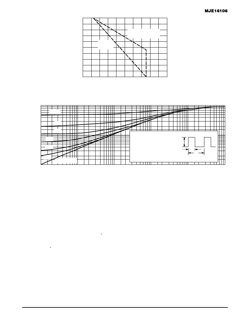
Figure 17. Power Derating
TC, CASE TEMPERATURE (
°
C)
Figure 18. Typical Thermal Response [Z
θ
JC(t)]
100
0
0
120
P
40
200
80
80
40
20
THERMAL
DERATING
60
160
SECOND BREAKDOWN
DERATING
0.02
0.01
SAFE OPERATING AREA INFORMATION
FORWARD BIAS
There are two limitations on the power handling ability of a
transistor: average junction temperature and second break-
down. Safe operating area curves indicate IC – VCE limits of
the transistor that must be observed for reliable operation;
i.e., the transistor must not be subjected to greater dissipa-
tion than the curves indicate.
The data in Figure 14 is based on TC = 25 C; TJ(pk) is
variable depending on power level. Second breakdown pulse
limits are valid for duty cycles to 10% but must be derated
when TC
≥
25 C. Second breakdown limitations do not
derate the same as thermal limitations. Allowable current at
the voltages shown on Figure 14 may be found at any case
temperature by using the appropriate curve on Figure 17.
TJ(pk) may be calculated from the data in Figure 18. At high
case temperatures, thermal limitations will reduce the power
that can be handled to values less than the limitations im-
posed by second breakdown.
REVERSE BIAS
For inductive loads, high voltage and high current must be
sustained simultaneously during turn–off, in most cases, with
the base–to–emitter junction reverse biased. Under these
conditions the collector voltage must be held to a safe level
at or below a specific value of collector current. This can be
accomplished by several means such as active clamping,
RC snubbing, load line shaping, etc. The safe level for these
devices is specified as Reverse Biased Safe Operating Area
and represents the voltage–current condition allowable dur-
ing reverse biased turn–off. This rating is verified under
clamped conditions so that the device is never subjected to
an avalanche mode. Figure 15 gives the RBSOA character-
istics.
SWITCHMODE III DESIGN CONSIDERATIONS
FBSOA
Allowable dc power dissipation in bipolar power transistors
decreases dramatically with increasing collector–emitter
voltage. A transistor which safely dissipates 100 watts at
10 volts will typically dissipate less than 10 watts at its rated
V(BR)CEO(sus). From a power handling point of view, current
and voltage are not interchangeable (see Application Note
AN875).
相关PDF资料 |
PDF描述 |
|---|---|
| MJE16204 | POWER TRANSISTORS 6.0 AMPERES 550 VOLTS-. VCES 45 AND 80 WATTS |
| MJE18604D2 | POWER TRANSISTORS 3 AMPERES 1600 VOLTS 100 WATTS |
| MJE18604 | POWER TRANSISTORS 3 AMPERES 1600 VOLTS 100 WATTS |
| MJE341 | 0.5 AMPERE POWER TRANSISTORS NPN SILICON 150-200 VOLTS 20 WATTS |
| MJE341 | POWER TRANSISTORS NPN SILICON |
相关代理商/技术参数 |
参数描述 |
|---|---|
| MJE16204 | 制造商:ON Semiconductor 功能描述:TRANSISTOR, NPN TO-220 |
| MJE170 | 功能描述:两极晶体管 - BJT 3A 40V 12.5W PNP RoHS:否 制造商:STMicroelectronics 配置: 晶体管极性:PNP 集电极—基极电压 VCBO: 集电极—发射极最大电压 VCEO:- 40 V 发射极 - 基极电压 VEBO:- 6 V 集电极—射极饱和电压: 最大直流电集电极电流: 增益带宽产品fT: 直流集电极/Base Gain hfe Min:100 A 最大工作温度: 安装风格:SMD/SMT 封装 / 箱体:PowerFLAT 2 x 2 |
| MJE170G | 功能描述:两极晶体管 - BJT 3A 40V 12.5W PNP RoHS:否 制造商:STMicroelectronics 配置: 晶体管极性:PNP 集电极—基极电压 VCBO: 集电极—发射极最大电压 VCEO:- 40 V 发射极 - 基极电压 VEBO:- 6 V 集电极—射极饱和电压: 最大直流电集电极电流: 增益带宽产品fT: 直流集电极/Base Gain hfe Min:100 A 最大工作温度: 安装风格:SMD/SMT 封装 / 箱体:PowerFLAT 2 x 2 |
| MJE170STU | 功能描述:两极晶体管 - BJT PNP Epitaxial Sil RoHS:否 制造商:STMicroelectronics 配置: 晶体管极性:PNP 集电极—基极电压 VCBO: 集电极—发射极最大电压 VCEO:- 40 V 发射极 - 基极电压 VEBO:- 6 V 集电极—射极饱和电压: 最大直流电集电极电流: 增益带宽产品fT: 直流集电极/Base Gain hfe Min:100 A 最大工作温度: 安装风格:SMD/SMT 封装 / 箱体:PowerFLAT 2 x 2 |
| MJE171 | 功能描述:两极晶体管 - BJT 3A 60V 12.5W PNP RoHS:否 制造商:STMicroelectronics 配置: 晶体管极性:PNP 集电极—基极电压 VCBO: 集电极—发射极最大电压 VCEO:- 40 V 发射极 - 基极电压 VEBO:- 6 V 集电极—射极饱和电压: 最大直流电集电极电流: 增益带宽产品fT: 直流集电极/Base Gain hfe Min:100 A 最大工作温度: 安装风格:SMD/SMT 封装 / 箱体:PowerFLAT 2 x 2 |
发布紧急采购,3分钟左右您将得到回复。