- 您现在的位置:买卖IC网 > PDF目录45334 > MM908E626AVEK (FREESCALE SEMICONDUCTOR INC) FLASH, 32 MHz, MICROCONTROLLER, PDSO54 PDF资料下载
参数资料
| 型号: | MM908E626AVEK |
| 厂商: | FREESCALE SEMICONDUCTOR INC |
| 元件分类: | 微控制器/微处理器 |
| 英文描述: | FLASH, 32 MHz, MICROCONTROLLER, PDSO54 |
| 封装: | 5.10 X 10.30 MM, 0.65 MM PITCH, LEAD FREE, SOIC-54 |
| 文件页数: | 34/43页 |
| 文件大小: | 842K |
| 代理商: | MM908E626AVEK |
第1页第2页第3页第4页第5页第6页第7页第8页第9页第10页第11页第12页第13页第14页第15页第16页第17页第18页第19页第20页第21页第22页第23页第24页第25页第26页第27页第28页第29页第30页第31页第32页第33页当前第34页第35页第36页第37页第38页第39页第40页第41页第42页第43页
Analog Integrated Circuit Device Data
4
Freescale Semiconductor
908E626
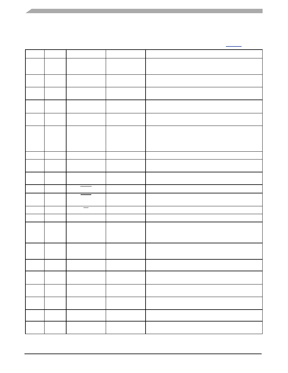
PIN CONNECTIONS
–
14, 21, 22,
28, 33, 35,
36, 37, 39
NC
No Connect
Not connected.
MCU
42
PTE1/RXD
Port E I/O
This pin is a special function, bidirectional I/O port pin that can is
shared with other functional modules in the MCU.
MCU
43
48
VREFL
VREFH
ADC References
These pins are the reference voltage pins for the analog-to-digital
converter (ADC).
MCU
44
47
VSSA
VDDA
ADC Supply Pins
These pins are the power supply pins for the analog-to-digital
converter.
MCU
45
46
EVSS
EVDD
MCU Power Supply
Pins
These pins are the ground and power supply pins, respectively. The
MCU operates from a single power supply.
MCU
49
50
52
53
54
PTA4/KBD4
PTA3/KBD3
PTA2/KBD2
PTA1/KBD1
PTA0/KBD0
Port A I/Os
These pins are special function, bidirectional I/O port pins that are
shared with other functional modules in the MCU.
MCU
51
FLSVPP
Test Pin
For test purposes only. Do not connect in the application.
Analog
15
FGEN
Current Limitation
Frequency Input
This is the input pin for the half-bridge current limitation PWM
frequency.
Analog
16
BEMF
Back Electromagnetic
Force Output
This pin gives the user information about back electromagnetic force
(BEMF).
Analog
17
RST_A
Internal Reset
This pin is the bidirectional reset pin of the analog die.
Analog
18
IRQ_A
Internal Interrupt
Output
This pin is the interrupt output pin of the analog die indicating errors
or wake-up events.
Analog
19
SS
Slave Select
This pin is the SPI slave select pin for the analog chip.
Analog
20
LIN
LIN Bus
This pin represents the single-wire bus transmitter and receiver.
Analog
23
26
29
32
HB1
HB2
HB3
HB4
Half-bridge Outputs
This device includes power MOSFETs configured as four half-bridge
driver outputs. These outputs may be configured for step motor
drivers, DC motor drivers, or as high side and low side switches.
Analog
24
27
31
VSUP1
VSUP2
VSUP3
Power Supply Pins
These pins are device power supply pins.
Analog
25
30
GND1
GND2
Power Ground Pins
These pins are device power ground connections.
Analog
34
HVDD
Switchable VDD
Output
This pin is a switchable VDD output for driving resistive loads
requiring a regulated 5.0 V supply; e.g., 3 pin Hall-effect sensors.
Analog
38
VDD
Voltage Regulator
Output
The 5.0 V voltage regulator output pin is intended to supply the
embedded microcontroller.
Analog
40
VSS
Voltage Regulator
Ground
Ground pin for the connection of all non-power ground connections
(microcontroller and sensors).
Analog
41
RXD
LIN Transceiver
Output
This pin is the output of LIN transceiver.
–
EP
Exposed Pad
The exposed pad pin on the bottom side of the package conducts
heat from the chip to the PCB board.
Table 1. 908E626 PIN DEFINITIONS
A functional description of each pin can be found in the Functional Pin Description section beginning on page 15.
Die
Pin
Pin Name
Formal Name
Definition
相关PDF资料 |
PDF描述 |
|---|---|
| MMAD1108R2 | 0.4 A, 8 ELEMENT, SILICON, SIGNAL DIODE |
| MMBD1504A-TP | 0.2 A, 2 ELEMENT, SILICON, SIGNAL DIODE |
| MMBD1505A-TP | 0.2 A, 2 ELEMENT, SILICON, SIGNAL DIODE |
| MMBD2837LT3 | 0.15 A, 2 ELEMENT, SILICON, SIGNAL DIODE, TO-236AB |
| MMBZ27VCL/DG | TVS DIODE, TO-236AB |
相关代理商/技术参数 |
参数描述 |
|---|---|
| MM908E626AVPEK | 功能描述:8位微控制器 -MCU MCU + LIN + MOTOR DRIVER RoHS:否 制造商:Silicon Labs 核心:8051 处理器系列:C8051F39x 数据总线宽度:8 bit 最大时钟频率:50 MHz 程序存储器大小:16 KB 数据 RAM 大小:1 KB 片上 ADC:Yes 工作电源电压:1.8 V to 3.6 V 工作温度范围:- 40 C to + 105 C 封装 / 箱体:QFN-20 安装风格:SMD/SMT |
| MM908E626AVPEKR2 | 功能描述:8位微控制器 -MCU RoHS:否 制造商:Silicon Labs 核心:8051 处理器系列:C8051F39x 数据总线宽度:8 bit 最大时钟频率:50 MHz 程序存储器大小:16 KB 数据 RAM 大小:1 KB 片上 ADC:Yes 工作电源电压:1.8 V to 3.6 V 工作温度范围:- 40 C to + 105 C 封装 / 箱体:QFN-20 安装风格:SMD/SMT |
| MM908E626R2 | 制造商:FREESCALE 制造商全称:Freescale Semiconductor, Inc 功能描述:Integrated Stepper Motor Driver with Embedded MCU and LIN Serial Communication |
| MM-90N | 功能描述:ANT MAGN MNT VEHIC 3.5"DIA 10'NF RoHS:是 类别:RF/IF 和 RFID >> RF 天线 系列:* 标准包装:1 系列:* |
| MM90R9F | 制造商:Ohmite Mfg Co 功能描述: |
发布紧急采购,3分钟左右您将得到回复。