- 您现在的位置:买卖IC网 > PDF目录95978 > MMDF3N03HDR2 (MOTOROLA INC) 2.8 A, 30 V, 0.09 ohm, 2 CHANNEL, N-CHANNEL, Si, POWER, MOSFET PDF资料下载
参数资料
| 型号: | MMDF3N03HDR2 |
| 厂商: | MOTOROLA INC |
| 元件分类: | JFETs |
| 英文描述: | 2.8 A, 30 V, 0.09 ohm, 2 CHANNEL, N-CHANNEL, Si, POWER, MOSFET |
| 封装: | SO-8 |
| 文件页数: | 5/10页 |
| 文件大小: | 281K |
| 代理商: | MMDF3N03HDR2 |
MMDF3N03HD
4
Motorola TMOS Power MOSFET Transistor Device Data
POWER MOSFET SWITCHING
Switching behavior is most easily modeled and predicted
by recognizing that the power MOSFET is charge controlled.
The lengths of various switching intervals (
t) are deter-
mined by how fast the FET input capacitance can be charged
by current from the generator.
The published capacitance data is difficult to use for calculat-
ing rise and fall because drain–gate capacitance varies
greatly with applied voltage. Accordingly, gate charge data is
used. In most cases, a satisfactory estimate of average input
current (IG(AV)) can be made from a rudimentary analysis of
the drive circuit so that
t = Q/IG(AV)
During the rise and fall time interval when switching a resis-
tive load, VGS remains virtually constant at a level known as
the plateau voltage, VSGP. Therefore, rise and fall times may
be approximated by the following:
tr = Q2 x RG/(VGG – VGSP)
tf = Q2 x RG/VGSP
where
VGG = the gate drive voltage, which varies from zero to VGG
RG = the gate drive resistance
and Q2 and VGSP are read from the gate charge curve.
During the turn–on and turn–off delay times, gate current is
not constant. The simplest calculation uses appropriate val-
ues from the capacitance curves in a standard equation for
voltage change in an RC network. The equations are:
td(on) = RG Ciss In [VGG/(VGG – VGSP)]
td(off) = RG Ciss In (VGG/VGSP)
The capacitance (Ciss) is read from the capacitance curve at
a voltage corresponding to the off–state condition when cal-
culating td(on) and is read at a voltage corresponding to the
on–state when calculating td(off).
At high switching speeds, parasitic circuit elements com-
plicate the analysis. The inductance of the MOSFET source
lead, inside the package and in the circuit wiring which is
common to both the drain and gate current paths, produces a
voltage at the source which reduces the gate drive current.
The voltage is determined by Ldi/dt, but since di/dt is a func-
tion of drain current, the mathematical solution is complex.
The MOSFET output capacitance also complicates the
mathematics. And finally, MOSFETs have finite internal gate
resistance which effectively adds to the resistance of the
driving source, but the internal resistance is difficult to mea-
sure and, consequently, is not specified.
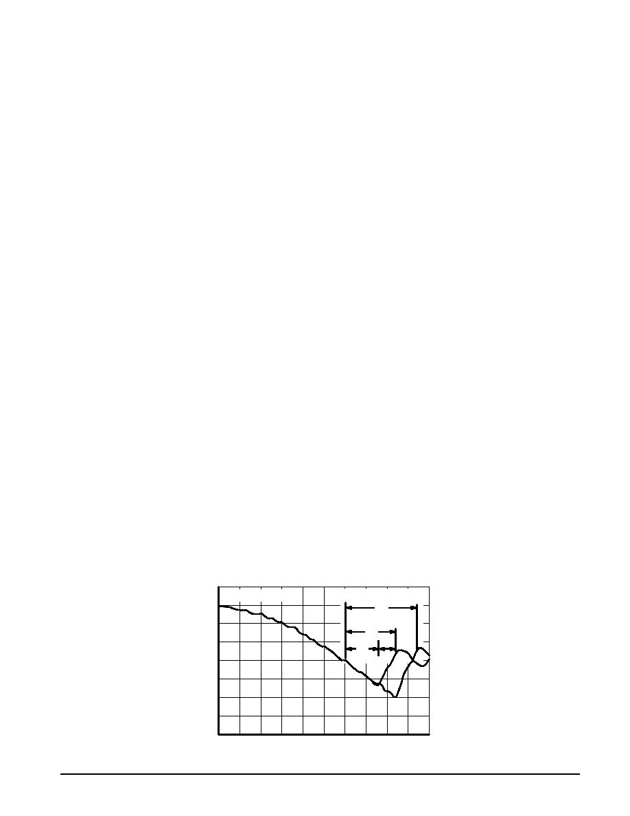
DRAIN–TO–SOURCE DIODE CHARACTERISTICS
The switching characteristics of a MOSFET body diode
are very important in systems using it as a freewheeling or
commutating diode. Of particular interest are the reverse re-
covery characteristics which play a major role in determining
switching losses, radiated noise, EMI and RFI.
System switching losses are largely due to the nature of
the body diode itself. The body diode is a minority carrier de-
vice, therefore it has a finite reverse recovery time, trr, due to
the storage of minority carrier charge, QRR, as shown in the
typical reverse recovery wave form of Figure 11. It is this
stored charge that, when cleared from the diode, passes
through a potential and defines an energy loss. Obviously,
repeatedly forcing the diode through reverse recovery further
increases switching losses. Therefore, one would like a
diode with short trr and low QRR specifications to minimize
these losses.
The abruptness of diode reverse recovery effects the
amount of radiated noise, voltage spikes, and current ring-
ing. The mechanisms at work are finite irremovable circuit
parasitic inductances and capacitances acted upon by high
di/dts. The diode’s negative di/dt during ta is directly con-
trolled by the device clearing the stored charge. However,
the positive di/dt during tb is an uncontrollable diode charac-
teristic and is usually the culprit that induces current ringing.
Therefore, when comparing diodes, the ratio of tb/ta serves
as a good indicator of recovery abruptness and thus gives a
comparative estimate of probable noise generated. A ratio of
1 is considered ideal and values less than 0.5 are considered
snappy.
Compared to Motorola standard cell density low voltage
MOSFETs, high cell density MOSFET diodes are faster
(shorter trr), have less stored charge and a softer reverse re-
covery characteristic. The softness advantage of the high
cell density diode means they can be forced through reverse
recovery at a higher di/dt than a standard cell MOSFET
diode without increasing the current ringing or the noise gen-
erated. In addition, power dissipation incurred from switching
the diode will be less due to the shorter recovery time and
lower switching losses.
I S
,SOURCE
CURRENT
t, TIME
Figure 7. Reverse Recovery Time (trr)
di/dt = 300 A/
s
Standard Cell Density
High Cell Density
tb
trr
ta
trr
相关PDF资料 |
PDF描述 |
|---|---|
| MMDF3N06VLR2 | 3.3 A, 60 V, 0.13 ohm, 2 CHANNEL, N-CHANNEL, Si, POWER, MOSFET |
| MMDF3P03HDR2 | 3000 mA, 30 V, 2 CHANNEL, P-CHANNEL, Si, SMALL SIGNAL, MOSFET |
| MMDF4N01ZR1 | 4500 mA, 20 V, 2 CHANNEL, N-CHANNEL, Si, SMALL SIGNAL, MOSFET |
| MMDF4N01ZR2 | 4500 mA, 20 V, 2 CHANNEL, N-CHANNEL, Si, SMALL SIGNAL, MOSFET |
| MMDF5N02ZR2 | 5000 mA, 20 V, 2 CHANNEL, N-CHANNEL, Si, SMALL SIGNAL, MOSFET |
相关代理商/技术参数 |
参数描述 |
|---|---|
| MMDF3N04HD | 制造商:ONSEMI 制造商全称:ON Semiconductor 功能描述:Power MOSFET 3 Amps, 40 Volts |
| MMDF3N04HDR2 | 功能描述:MOSFET 40V 3A N-Channel RoHS:否 制造商:STMicroelectronics 晶体管极性:N-Channel 汲极/源极击穿电压:650 V 闸/源击穿电压:25 V 漏极连续电流:130 A 电阻汲极/源极 RDS(导通):0.014 Ohms 配置:Single 最大工作温度: 安装风格:Through Hole 封装 / 箱体:Max247 封装:Tube |
| MMDF3N04HDR2G | 功能描述:MOSFET NFET SO8D 40V 3.4A 80mOhm RoHS:否 制造商:STMicroelectronics 晶体管极性:N-Channel 汲极/源极击穿电压:650 V 闸/源击穿电压:25 V 漏极连续电流:130 A 电阻汲极/源极 RDS(导通):0.014 Ohms 配置:Single 最大工作温度: 安装风格:Through Hole 封装 / 箱体:Max247 封装:Tube |
| MMDF3N06HD | 制造商:MOTOROLA 制造商全称:Motorola, Inc 功能描述:DUAL TMOS POWER MOSFET 60 VOLTS |
| MMDF3N06VL | 制造商:ONSEMI 制造商全称:ON Semiconductor 功能描述:Power MOSFET 3 Amps, 60 Volts N−Channel SO−8, Dual |
发布紧急采购,3分钟左右您将得到回复。