- 您现在的位置:买卖IC网 > Datasheet目录478 > MMDF3N04HDR2G (ON Semiconductor)MOSFET N-CH DUAL 3.4A 40V 8SOIC Datasheet资料下载
参数资料
| 型号: | MMDF3N04HDR2G |
| 厂商: | ON Semiconductor |
| 文件页数: | 5/8页 |
| 文件大小: | 0K |
| 描述: | MOSFET N-CH DUAL 3.4A 40V 8SOIC |
| 产品变化通告: | Product Obsolescence 14/Apr/2010 |
| 产品目录绘图: | MOSFET 8-SOIC |
| 标准包装: | 10 |
| FET 型: | 2 个 N 沟道(双) |
| FET 特点: | 逻辑电平门 |
| 漏极至源极电压(Vdss): | 40V |
| 电流 - 连续漏极(Id) @ 25° C: | 3.4A |
| 开态Rds(最大)@ Id, Vgs @ 25° C: | 80 毫欧 @ 3.4A,10V |
| Id 时的 Vgs(th)(最大): | 3V @ 250µA |
| 闸电荷(Qg) @ Vgs: | 28nC @ 10V |
| 输入电容 (Ciss) @ Vds: | 900pF @ 32V |
| 功率 - 最大: | 1.39W |
| 安装类型: | 表面贴装 |
| 封装/外壳: | 8-SOIC(0.154",3.90mm 宽) |
| 供应商设备封装: | 8-SOICN |
| 包装: | 标准包装 |
| 其它名称: | MMDF3N04HDR2GOSDKR |
�� �
�
�MMDF3N04HD�
�12�
�QT�
�40�
�1000�
�V� DD� =� 20� V�
�I� D� =� 3.4� A�
�9�
�30�
�100�
�V� GS� =� 10� V�
�T� J� =� 25� °� C�
�6�
�V� DS�
�V� GS�
�20�
�t� d(off)�
�t� f�
�3�
�Q1�
�Q2�
�I� D� =� 3.4� A�
�T� J� =� 25� °� C�
�10�
�10�
�t� r�
�t� d(on)�
�Q3�
�0�
�0�
�4�
�8�
�12�
�0�
�16�
�1�
�1�
�10�
�100�
�Q� g� ,� TOTAL� GATE� CHARGE� (nC)�
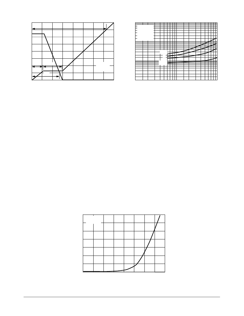
�Figure� 8.� Gate� ?� To� ?� Source� and� Drain� ?� To� ?� Source�
�Voltage� versus� Total� Charge�
�R� G� ,� GATE� RESISTANCE� (OHMS)�
�Figure� 9.� Resistive� Switching� Time�
�Variation� versus� Gate� Resistance�
�DRAIN� ?� TO� ?� SOURCE� DIODE� CHARACTERISTICS�
�The� switching� characteristics� of� a� MOSFET� body� diode�
�are� very� important� in� systems� using� it� as� a� freewheeling� or�
�commutating� diode.� Of� particular� interest� are� the� reverse�
�recovery� characteristics� which� play� a� major� role� in�
�determining� switching� losses,� radiated� noise,� EMI� and� RFI.�
�System� switching� losses� are� largely� due� to� the� nature� of�
�the� body� diode� itself.� The� body� diode� is� a� minority� carrier�
�device,� therefore� it� has� a� finite� reverse� recovery� time,� t� rr� ,� due�
�to� the� storage� of� minority� carrier� charge,� Q� RR� ,� as� shown� in�
�the� typical� reverse� recovery� wave� form� of� Figure� 12.� It� is� this�
�stored� charge� that,� when� cleared� from� the� diode,� passes�
�through� a� potential� and� defines� an� energy� loss.� Obviously,�
�repeatedly� forcing� the� diode� through� reverse� recovery�
�further� increases� switching� losses.� Therefore,� one� would�
�like� a� diode� with� short� t� rr� and� low� Q� RR� specifications� to�
�minimize� these� losses.�
�The� abruptness� of� diode� reverse� recovery� effects� the�
�amount� of� radiated� noise,� voltage� spikes,� and� current�
�ringing.� The� mechanisms� at� work� are� finite� irremovable�
�circuit� parasitic� inductances� and� capacitances� acted� upon� by�
�high� di/dts.� The� diode’s� negative� di/dt� during� t� a� is� directly�
�controlled� by� the� device� clearing� the� stored� charge.�
�However,� the� positive� di/dt� during� t� b� is� an� uncontrollable�
�diode� characteristic� and� is� usually� the� culprit� that� induces�
�current� ringing.� Therefore,� when� comparing� diodes,� the�
�ratio� of� t� b� /t� a� serves� as� a� good� indicator� of� recovery�
�abruptness� and� thus� gives� a� comparative� estimate� of�
�probable� noise� generated.� A� ratio� of� 1� is� considered� ideal� and�
�values� less� than� 0.5� are� considered� snappy.�
�Compared� to� ON� Semiconductor� standard� cell� density�
�low� voltage� MOSFETs,� high� cell� density� MOSFET� diodes�
�are� faster� (shorter� t� rr� ),� have� less� stored� charge� and� a� softer�
�reverse� recovery� characteristic.� The� softness� advantage� of�
�the� high� cell� density� diode� means� they� can� be� forced� through�
�reverse� recovery� at� a� higher� di/dt� than� a� standard� cell�
�MOSFET� diode� without� increasing� the� current� ringing� or� the�
�noise� generated.� In� addition,� power� dissipation� incurred�
�from� switching� the� diode� will� be� less� due� to� the� shorter�
�recovery� time� and� lower� switching� losses.�
�3.5�
�3.0�
�2.5�
�2.0�
�1.5�
�1.0�
�0.5�
�T� J� =� 25� °� C�
�V� GS� =� 0� V�
�0�
�0.5�
�0.55�
�0.6� 0.65� 0.7� 0.75� 0.8� 0.85�
�0.9�
�V� SD� ,� SOURCE-TO-DRAIN� VOLTAGE� (VOLTS)�
�Figure� 10.� Diode� Forward� Voltage� versus� Current�
�http://onsemi.com�
�5�
�相关PDF资料 |
PDF描述 |
|---|---|
| MMDFS6N303R2 | MOSFET N-CH 30V 6A 8-SOIC |
| MMFT5P03HDT1 | MOSFET P-CH 30V 3.7A SOT223 |
| MMFT960T1 | MOSFET N-CH 60V 300MA SOT223 |
| MMG3002NT1 | IC AMP RF GP 3600MHZ 5.2V SOT-89 |
| MMG3006NT1 | TRANS GPA 33DBM 16-QFN |
相关代理商/技术参数 |
参数描述 |
|---|---|
| MMDF3N06HD | 制造商:MOTOROLA 制造商全称:Motorola, Inc 功能描述:DUAL TMOS POWER MOSFET 60 VOLTS |
| MMDF3N06VL | 制造商:ONSEMI 制造商全称:ON Semiconductor 功能描述:Power MOSFET 3 Amps, 60 Volts N−Channel SO−8, Dual |
| MMDF3N06VLR2 | 制造商:ON Semiconductor 功能描述:Trans MOSFET N-CH 60V 3.3A 8-Pin SOIC N T/R |
| MMDF3NO2HD | 制造商:MOTOROLA 制造商全称:Motorola, Inc 功能描述:TMOS DUAL N-CHANNEL FIELD EFFECT TRANSISTOR |
| MMDF3P03HD | 制造商:MOTOROLA 制造商全称:Motorola, Inc 功能描述:DUAL TMOS POWER MOSFET 30 VOLTS |
发布紧急采购,3分钟左右您将得到回复。