- 您现在的位置:买卖IC网 > PDF目录45353 > MPC745BPX350LE (FREESCALE SEMICONDUCTOR INC) 32-BIT, 350 MHz, RISC PROCESSOR, PBGA255 PDF资料下载
参数资料
| 型号: | MPC745BPX350LE |
| 厂商: | FREESCALE SEMICONDUCTOR INC |
| 元件分类: | 微控制器/微处理器 |
| 英文描述: | 32-BIT, 350 MHz, RISC PROCESSOR, PBGA255 |
| 封装: | 21 X 21 MM, 2.80 MM HEIGHT, 1.27 MM PITCH, PLASTIC, BGA-255 |
| 文件页数: | 10/60页 |
| 文件大小: | 1559K |
| 代理商: | MPC745BPX350LE |
第1页第2页第3页第4页第5页第6页第7页第8页第9页当前第10页第11页第12页第13页第14页第15页第16页第17页第18页第19页第20页第21页第22页第23页第24页第25页第26页第27页第28页第29页第30页第31页第32页第33页第34页第35页第36页第37页第38页第39页第40页第41页第42页第43页第44页第45页第46页第47页第48页第49页第50页第51页第52页第53页第54页第55页第56页第57页第58页第59页第60页
MPC755 RISC Microprocessor Hardware Specifications, Rev. 7.0
18
Freescale Semiconductor
Electrical and Thermal Characteristics
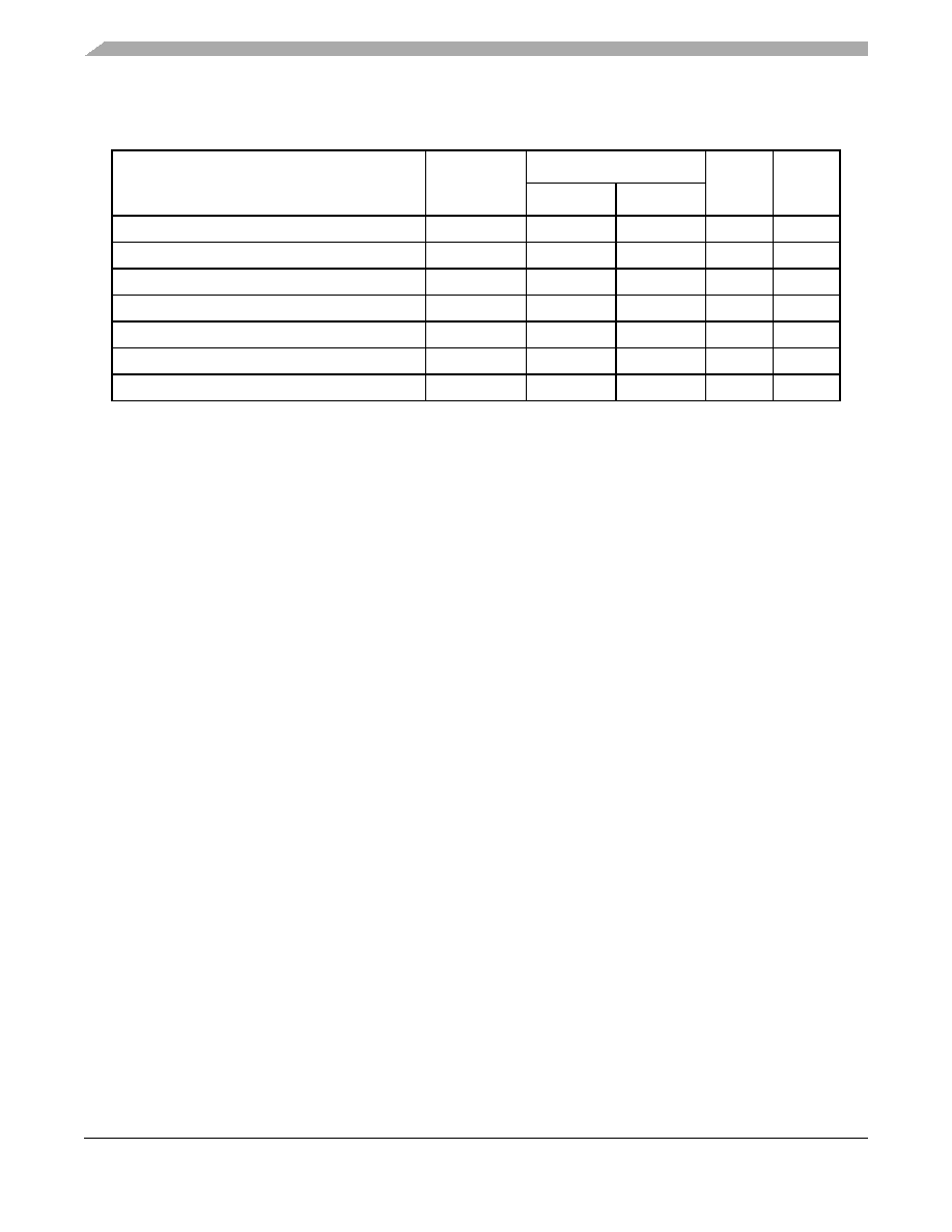
Table 11. L2CLK Output AC Timing Specification
At recommended operating conditions (see Table 3)
Parameter
Symbol
All Speed Grades
Unit
Notes
Min
Max
L2CLK frequency
fL2CLK
80
450
MHz
1, 4
L2CLK cycle time
tL2CLK
2.5
12.5
ns
L2CLK duty cycle
tCHCL/tL2CLK
45
55
%
2, 7
Internal DLL-relock time
640
—
L2CLK
3, 7
DLL capture window
0
10
ns
5, 7
L2CLK_OUT output-to-output skew
tL2CSKW
—50
ps
6, 7
L2CLK_OUT output jitter
—
±150
ps
6, 7
Notes:
1. L2CLK outputs are L2CLK_OUTA, L2CLK_OUTB, L2CLK_OUT, and L2SYNC_OUT pins. The L2CLK
frequency-to-core frequency settings must be chosen such that the resulting L2CLK frequency and core frequency
do not exceed their respective maximum or minimum operating frequencies. The maximum L2LCK frequency will
be system dependent. L2CLK_OUTA and L2CLK_OUTB must have equal loading.
2. The nominal duty cycle of the L2CLK is 50% measured at midpoint voltage.
3. The DLL-relock time is specified in terms of L2CLK periods. The number in the table must be multiplied by the period
of L2CLK to compute the actual time duration in ns. Relock timing is guaranteed by design and characterization.
4. The L2CR[L2SL] bit should be set for L2CLK frequencies less than 110 MHz. This adds more delay to each tap of
the DLL.
5. Allowable skew between L2SYNC_OUT and L2SYNC_IN.
6. This output jitter number represents the maximum delay of one tap forward or one tap back from the current DLL
tap as the phase comparator seeks to minimize the phase difference between L2SYNC_IN and the internal L2CLK.
This number must be comprehended in the L2 timing analysis. The input jitter on SYSCLK affects L2CLK_OUT and
the L2 address/data/control signals equally and, therefore, is already comprehended in the AC timing and does not
have to be considered in the L2 timing analysis.
7. Guaranteed by design.
相关PDF资料 |
PDF描述 |
|---|---|
| MPC755BPX350LE | 32-BIT, 350 MHz, RISC PROCESSOR, PBGA360 |
| MPC755CPX400LE | 32-BIT, 400 MHz, RISC PROCESSOR, PBGA360 |
| MPC745BVT300LE | 32-BIT, 300 MHz, RISC PROCESSOR, PBGA255 |
| MPC755BVT300LE | 32-BIT, 300 MHz, RISC PROCESSOR, PBGA360 |
| MPC823ZC25 | 32-BIT, RISC PROCESSOR, PBGA256 |
相关代理商/技术参数 |
参数描述 |
|---|---|
| MPC745BVT300LE | 功能描述:微处理器 - MPU GF REV2.8105C RoHS:否 制造商:Atmel 处理器系列:SAMA5D31 核心:ARM Cortex A5 数据总线宽度:32 bit 最大时钟频率:536 MHz 程序存储器大小:32 KB 数据 RAM 大小:128 KB 接口类型:CAN, Ethernet, LIN, SPI,TWI, UART, USB 工作电源电压:1.8 V to 3.3 V 最大工作温度:+ 85 C 安装风格:SMD/SMT 封装 / 箱体:FBGA-324 |
| MPC745BVT350LE | 功能描述:微处理器 - MPU GF REV2.8105C RoHS:否 制造商:Atmel 处理器系列:SAMA5D31 核心:ARM Cortex A5 数据总线宽度:32 bit 最大时钟频率:536 MHz 程序存储器大小:32 KB 数据 RAM 大小:128 KB 接口类型:CAN, Ethernet, LIN, SPI,TWI, UART, USB 工作电源电压:1.8 V to 3.3 V 最大工作温度:+ 85 C 安装风格:SMD/SMT 封装 / 箱体:FBGA-324 |
| MPC745CPX350LE | 功能描述:微处理器 - MPU GF REV 2.8 105C 6W RoHS:否 制造商:Atmel 处理器系列:SAMA5D31 核心:ARM Cortex A5 数据总线宽度:32 bit 最大时钟频率:536 MHz 程序存储器大小:32 KB 数据 RAM 大小:128 KB 接口类型:CAN, Ethernet, LIN, SPI,TWI, UART, USB 工作电源电压:1.8 V to 3.3 V 最大工作温度:+ 85 C 安装风格:SMD/SMT 封装 / 箱体:FBGA-324 |
| MPC745CPX350LE | 制造商:Freescale Semiconductor 功能描述:IC 32-BIT MPU 350MHZ 255-FCPBGA |
| MPC745CVT350LE | 功能描述:微处理器 - MPU GF REV2.8@6W RoHS:否 制造商:Atmel 处理器系列:SAMA5D31 核心:ARM Cortex A5 数据总线宽度:32 bit 最大时钟频率:536 MHz 程序存储器大小:32 KB 数据 RAM 大小:128 KB 接口类型:CAN, Ethernet, LIN, SPI,TWI, UART, USB 工作电源电压:1.8 V to 3.3 V 最大工作温度:+ 85 C 安装风格:SMD/SMT 封装 / 箱体:FBGA-324 |
发布紧急采购,3分钟左右您将得到回复。